Color active matrix type vertically aligned mode liquid crystal display and driving method thereof

a vertical alignment mode, liquid crystal display technology, applied in static indicating devices, non-linear optics, instruments, etc., can solve the problems of difficulty in shortening the process, inability to use dry ashing methods using oxygen plasma, and unavoidable cost increases, so as to improve reduce the cost of polarizing plates. , the effect of improving the effective use efficiency of polarizing plates

Inactive Publication Date: 2009-04-09
OBAYASHISEIKOU CO LTD
View PDF2 Cites 22 Cited by
  • Summary
  • Abstract
  • Description
  • Claims
  • Application Information

AI Technical Summary

Benefits of technology

[0068]Use of the methods 22, 23, 24, 25, 26, 30, 31, 32, and 33 may sharply improve effective use efficiency of a polarizing plate compared with conventional liquid crystal panels in TN (Twisted Nematic) mode, which may reduce a cost of a polarizing plate used in very large-sized liquid crystal displays. In addition, effective use efficiency of a polarizer having reflexibility comprising multilayer laminated body of two kinds of materials (brand name: DBEF by 3M Inc.) used for a backlight may also be sharply improved, which may also reduce a cost of a backlight for very large-sized liquid crystal displays.
[0069]Since use of the methods 22, 23, 24, 25, 34, and 35 enables manufacture of active matrix liquid crystal panels of the present invention using same processes, without changing most of conventional manufacturing processes of an active matrix substrate and manufacturing processes of a color filter in TN mode, leading to demonstration of predominancy in respect of yield and low cost.
[0070]Use of the methods 22, 23, 24, 25, 26, 36, 37, and 38 may realize vertically aligned mode liquid crystal display having a simplest structure. This method does not have excessive and unnecessary thin film transistor elements in one pixel, but an aperture ratio may be set large in the highest, being able to realize a bright display.
[0071]Since use of the methods 22, 23, 24, 25, 26, 27, 28, 29, and 39 enables impression of a large voltage between a transparent pixel electrode and a liquid crystal alignment direction control electrode, deformation of an electric field for driving vertically aligned liquid crystal molecules may be set significantly large. This may improve a rate of reaction of the liquid crystal molecules, and even in moving image displaying, a flow of image and a residual image phenomenon are scarcely generated.
[0072]When a scanning line of n row is set as OFF, use of the methods 22, 23, 24, 25, 40, and 41 may decrease a potential variation of a transparent pixel electrode, and reduce flicker.
[0073]Use of the methods 22, 23, 24, 25, and 26 may provide vertically aligned liquid crystal molecules with alignment almost perpendicular in all areas at the time of black display, which reduces light leakage more than in conventional methods using bumps, and may realize completely uniform black display also in a dark room.

Problems solved by technology

In conventional type multi-domain vertically aligned mode liquid crystal displays, it is necessary that bumps or slits are formed on the transparent common electrode in the color filter side substrate, which required one excessive photo mask process.
Therefore, in this conventional technology, cost increase is unavoidable.
Since bumps are made of positive type photoresists, perfect removal of organic solvents, and furthermore hardening by baking at high temperatures of no less than 200 degrees are furthermore required, leading difficulty in shortening the processes.
When contaminants are eluted out into liquid crystals from the bumps of positive type photoresists, a phenomenon of afterimage will occur, resulting in reliability problems.
In color filter substrates using the conventional bumps, positive type photoresists are used as materials for the bumps, and therefore, when a defect occurs in the application process of a vertical alignment film 6 and reworking is required, a dry ashing method using oxygen plasma can not be used.
Therefore, a wet remove method requiring high running cost using organic solvents has to be used, which causes a disadvantage requiring a very high reworking cost.
In vertically aligned mode liquid crystal displays using the conventional type bumps and slits, when a display switchovers to a half tone display from a black display, or to a half tone display from a white display, there arises defects that the liquid crystals operate in a slow response speed.

Method used


Image

  • Color active matrix type vertically aligned mode liquid crystal display and driving method thereof
  • Color active matrix type vertically aligned mode liquid crystal display and driving method thereof
  • Color active matrix type vertically aligned mode liquid crystal display and driving method thereof

Examples


example 1

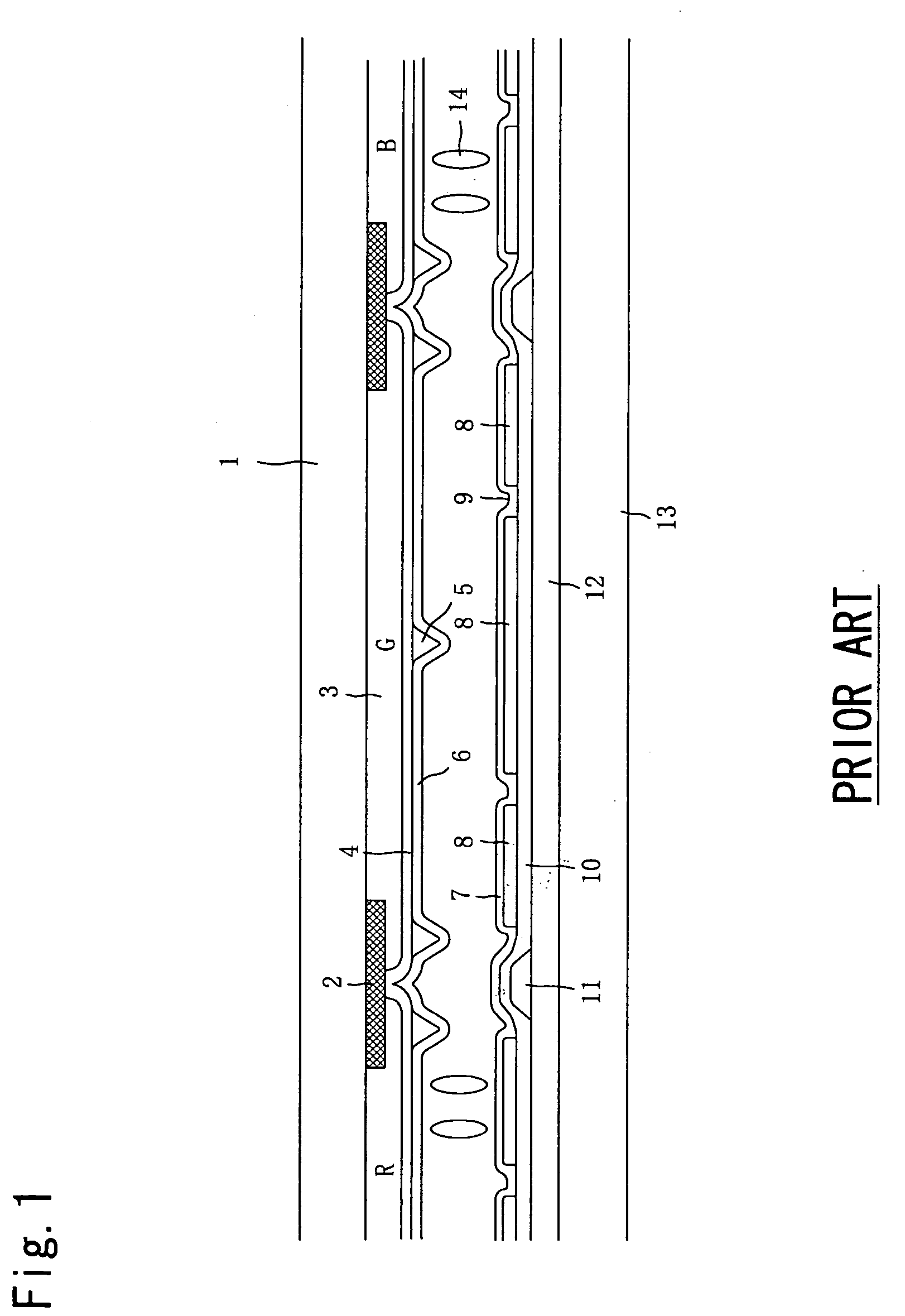
[0176]FIGS. 4, 5, and 6 show sectional views of Example 1 of the present invention. A color filter substrate 1 has a flat transparent common electrode 4, and an active matrix substrate 13 is arranged facing the substrate 1 and in parallel.

[0177]In the active matrix substrate 13, firstly, a scan signal wiring 17 and a liquid crystal alignment direction control electrode 15 are simultaneously formed in the same layer, and subsequently, a gate insulator film 12, an amorphous silicone layer, and an n+ amorphous silicone layer for ohmic contacts are deposited.

[0178]After formation of a thin film transistor element part, a video signal wiring 11 and a drain electrode are formed.

[0179]Next, a contact hole 18 is formed in a portion of a drain electrode after deposition of a passivation film 10, and then a transparent electric conductive film is deposited. In the transparent electric conductive film, as shown in FIG. 7, some slits are formed and each pixel is completely separated for every p...

example 2

[0183]FIG. 30, FIG. 31, and FIG. 32 show sectional views of Example 2 of the present invention. In fundamental aspect, almost the same structure as in Example 1 is used for Example 2. An electrode structure of the Example has special features that two kinds of electrode structures as shown in FIG. 2 and FIG. 3 exist together in one pixel.

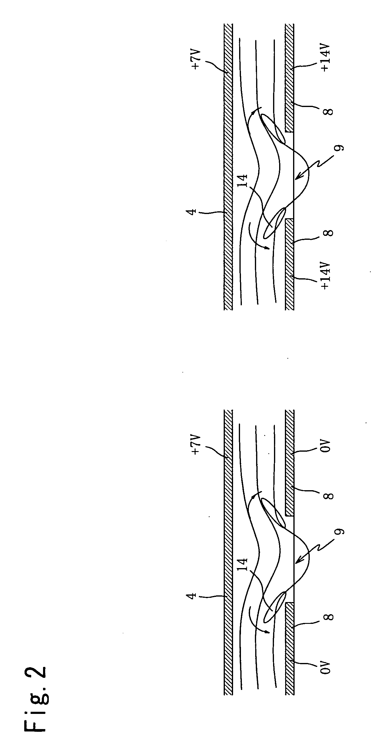
[0184]As shown in FIG. 30, FIG. 31, and FIG. 32, since a video signal wiring 11 is only sandwiched by transparent pixel electrodes 8 from both of right and left sides, capacitance of a video signal wiring 11 can be designed minimal, and accordingly, even if a resistance of the video signal wiring 11 is high, a problem of signal delay is hard to be generated.

[0185]FIG. 24 shows a plan view of Example 2. Only one row of liquid crystal alignment direction control electrode 15 exists in one pixel. Adjacent transparent pixel electrodes 8 are connected to a thin film transistor element 16 controlled by a different scan signal wiring 17, respectively.

[0186...

example 3

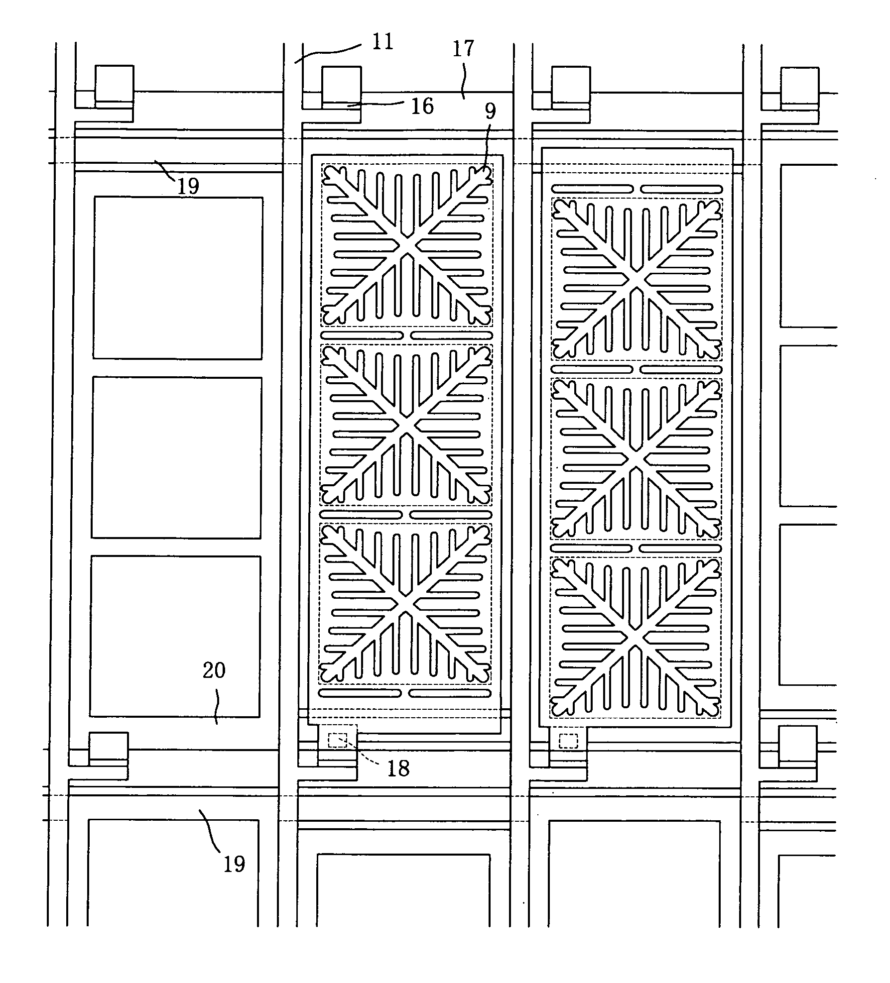
[0188]FIG. 7 shows a plan view of Example 3 of the present invention. The Example has a structure where two kinds of structures, a structure shown in a cross section structural figure of Example 1 and a structure shown in a cross section structural figure of Example 2, are mixed inside one pixel. In one pixel, two rows of liquid crystal alignment direction control electrodes of an upper liquid crystal alignment direction control electrode 19 and a lower liquid crystal alignment direction control electrode 20 are arranged, each potential is set as positive electrode potential and negative electrode potential on the basis of a potential of a countering flat common electrode 4 of a color filter side substrate. Adjacent transparent pixel electrodes 8 are controlled by a different liquid crystal alignment direction control electrode, respectively.

[0189]FIG. 11 and FIG. 12 show a transparent common electrode potential 21, a video signal wiring waveform 22 of odd number column, a scanning ...


PUM

PropertyMeasurementUnit
angleaaaaaaaaaa
dielectric constantaaaaaaaaaa

Abstract

A big screen display suitable for moving image displaying that has an excellent viewing angle property, an excellent reliability and a productivity, and a quick speed of response, and has a bright and excellent contrast is realized at low cost. Vertically aligned mode liquid crystal display comprises a scan wiring, a video signal wiring, a pixel electrode, an alignment directional control electrode, and a thin film transistor element formed in a position where a scan wiring and a video signal wiring intersect with each other, and a common electrode formed in opposing substrate side. An electric field distribution formed with three electrodes comprising an alignment directional control electrode, and a pixel electrode, and a common electrode formed in an countering substrate side may control motion directions of vertically aligned anisotropic liquid crystal molecules having a negative dielectric constant.

Description

FIELD OF THE INVENTION[0001]The present invention relates to a big screen active matrix type liquid crystal TV viewing display, and more particularly, to an active matrix type liquid crystal display having a wide viewing angle, high brightness, and a high response speed as well as low cost, and to a method for driving the display.BACKGROUND OF THE INVENTION[0002]As shown in FIG. 1, in conventional type vertically aligned mode liquid crystal displays, a mode is adopted in which bumps 5 for controlling a motion direction of liquid crystal molecules 14 are formed on a transparent common electrode 4 of a color filter side substrate 1, and slits 9 for controlling a motion direction of the liquid crystal molecules 14 are provided in transparent pixel electrodes 8 of an active matrix substrate 13, the bumps 5 and the slits 9 determine the motion direction of the liquid crystal molecules 14 serving as one set. There is also provided a method in which slits for controlling the motion directi...

Claims


Application Information

Patent Timeline
Patent Type & Authority Applications(United States)
IPC IPC(8): G09G3/36G02F1/133G02F1/1333G02F1/139
CPCG02F1/133707G02F1/1393G09G3/3648G09G3/3614G02F2201/128G02F1/133
Inventor HIROTA, NAOTO
Owner OBAYASHISEIKOU CO LTD
Why Eureka
Try Eureka