Semiconductor device and method of manufacturing the same

a semiconductor and field-effect transistor technology, applied in the direction of semiconductor devices, transistors, electrical appliances, etc., to achieve the effect of higher integration and higher performance of a semiconductor devi

Inactive Publication Date: 2009-04-16
RENESAS ELECTRONICS CORP
View PDF11 Cites 64 Cited by
  • Summary
  • Abstract
  • Description
  • Claims
  • Application Information

AI Technical Summary

Benefits of technology

[0016]An object of the present invention is to provide a technology capable of realizing higher integration and higher performance of a semiconductor device.

Problems solved by technology

Due to this phenomenon, after simply forming the elevated layers on both of the SOI-MISFET and the bulk-MISFET by the selective epitaxial growth, when the full silicidation processing is performed for fully siliciding the polycrystalline polysilicon of the gate up to the gate insulator, the problem described below is posed.

Method used


Image

  • Semiconductor device and method of manufacturing the same
  • Semiconductor device and method of manufacturing the same
  • Semiconductor device and method of manufacturing the same

Examples


first embodiment

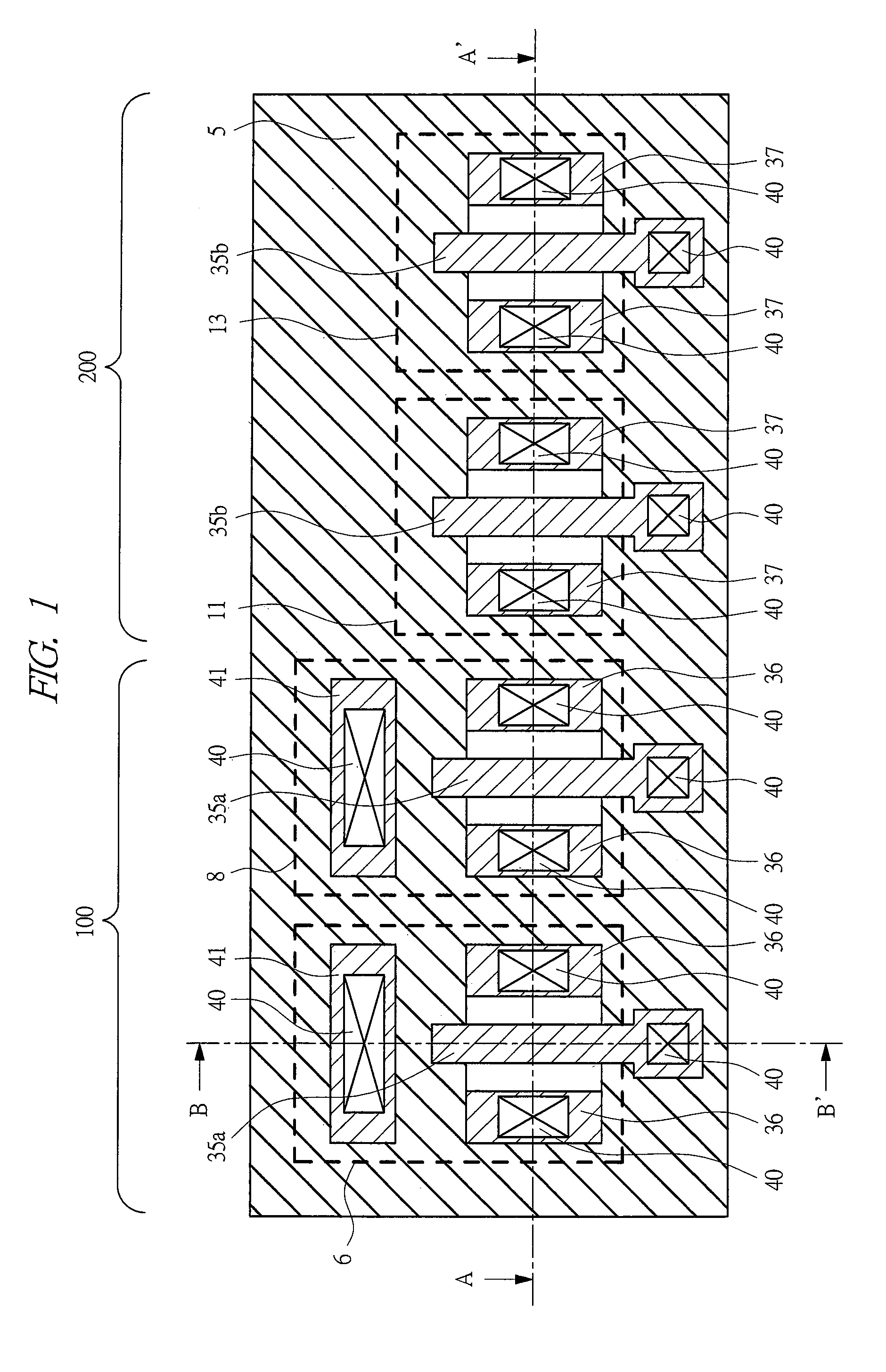
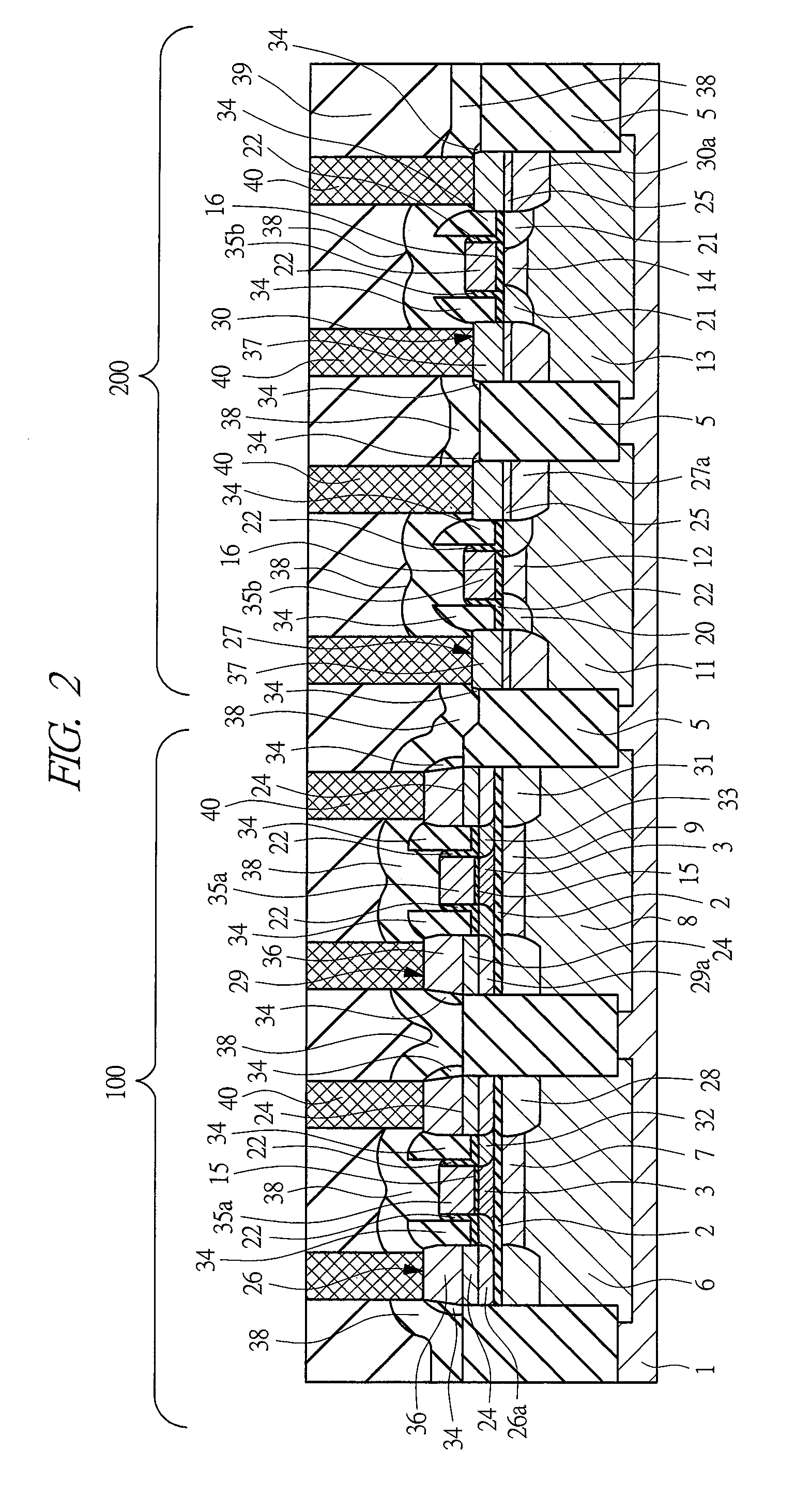
[0059]In FIGS. 1 to 3, a semiconductor device according to an embodiment of the present invention is shown. FIG. 1 is a planar view of main parts, FIG. 2 is a cross-sectional view of main parts taken along the line A-A′ of FIG. 1, and FIG. 3 is a cross-sectional view of main parts taken along the line B-B′ of FIG. 1. In the planar view of FIG. 1, to facilitate visualization, illustrations of part of members such as an insulating film (insulator) are omitted.

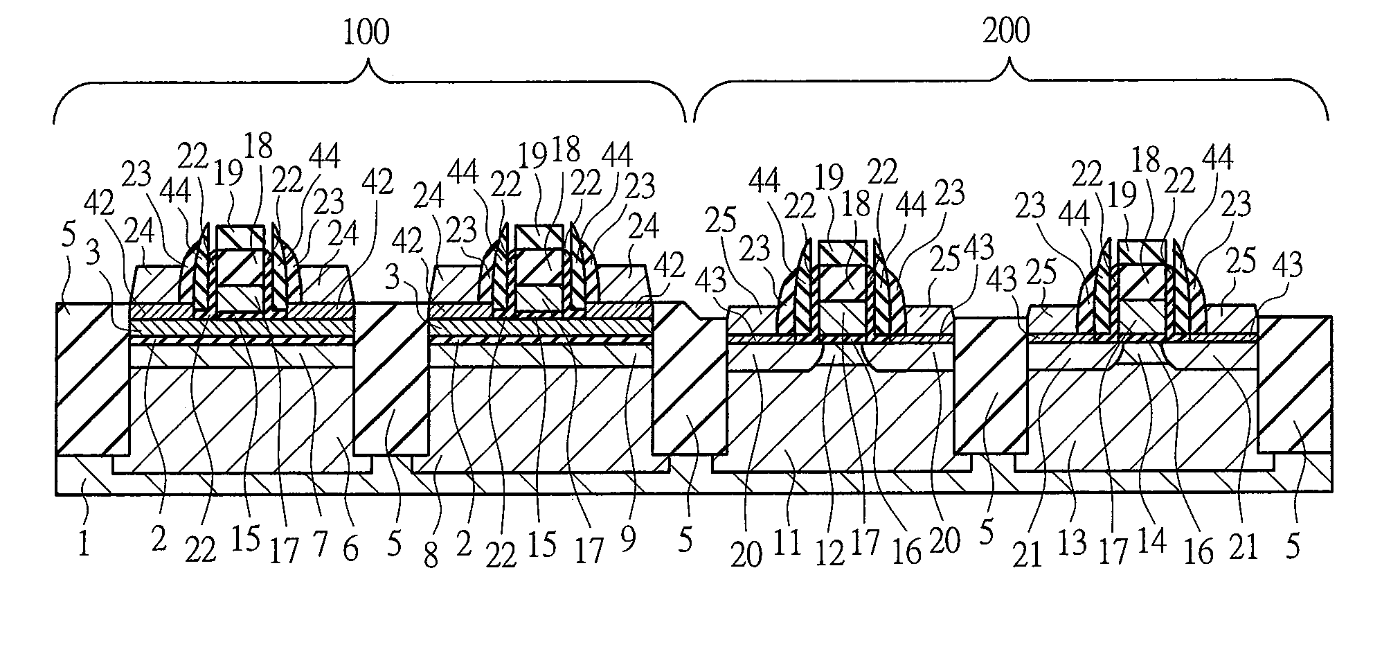
[0060]The semiconductor device of the present embodiment includes: an SOI-MISFET having a gate electrode 35a that is fully silicided and an elevated source and drain structure inside an SOI region 100 of a silicon substrate 1; and a bulk-MISFET (high-breakdown voltage MISFET) having a gate electrode 35b that is fully silicided and an elevated source and drain structure inside a bulk region 200 on the silicon substrate 1 that is exposed by removing an SOI layer 3 and a buried insulating layer 2.

[0061]In this manner, the semiconduc...

second embodiment

[0117]A plan view of main parts of a semiconductor device according to a second embodiment of the present invention is, for example, FIG. 1, and a cross-sectional view of main parts of a semiconductor substrate taken along the line A-A′ of FIG. 1 at this time is FIG. 24.

[0118]While the elevated layers of the SOI-MISFET and the bulk-MISFET have been formed by the single selective epitaxial growth process in the first embodiment, in the second embodiment, the selective epitaxial growth process is performed twice, thereby forming first and second elevated layers for the SOI-MISFET and the bulk-MISFET, respectively. This point is different from the first embodiment.

[0119]In the SOI-MISFET according to the second embodiment, a first elevated layer (lowermost layer) 42 is formed directly below the sidewalls 34 at both sides of the gate. Hence, the diffusion layers 26 and 29 are provided such that the two layers have a distance from the gate electrode 35a, the uppermost elevated layers 24 ...


PUM


Abstract

There is provided an SOI-MISFET including: an SOI layer; a gate electrode provided on the SOI layer interposing a gate insulator; and a first elevated layer provided higher in height from the SOI layer than the gate electrode at both sidewall sides of the gate electrode on the SOI layer so as to constitute a source and drain. Further, there is also provided a bulk-MISFET including: a gate electrode provided on a silicon substrate interposing a gate insulator thicker than the gate insulator of the SOI MISFET; and a second elevated layer configuring a source and drain provided on a semiconductor substrate at both sidewalls of the gate electrode. A the first elevated layer is thicker than the elevated layer, and the whole of the gate electrodes, part of the source and drain of the SOI-MISFET, and part of the source and drain of the bulk-MISFET are silicided.

Description

CROSS-REFERENCE TO RELATED APPLICATION[0001]The present application claims priority from Japanese Patent Application No. JP 2007-265037 filed on Oct. 11, 2007, the content of which is hereby incorporated by reference into this application.TECHNICAL FIELD OF THE INVENTION[0002]The present invention relates to a semiconductor device and a manufacturing technology thereof. More particularly, the present invention relates to a MISFET (Metal Insulator Semiconductor Field Effect Transistor) formed on a substrate (SOI substrate) having an SOI (Silicon on Insulator) structure.BACKGROUND OF THE INVENTION[0003]Accompanied with introduction of higher integration and higher performance of LSIs (semiconductor devices), the miniaturization of a MISFET constituting an LSI has been advanced, and as a gate length of the MISFET is scaled, and thus a problem of short channel effect that reduces a threshold voltage Vth has become significant. This short channel effect arises from the fact that the broa...

Claims


Application Information

Patent Timeline
Patent Type & Authority Applications(United States)
IPC IPC(8): H01L27/088H01L21/8234
CPCH01L21/26506H01L21/823418H01L21/823481H01L27/1203H01L21/823878H01L21/84H01L21/823814H01L21/26513H01L21/76283H01L27/1207
Inventor ISHIGAKI, TAKASHITSUCHIYA, RYUTAMORITA, YUSUKESUGII, NOBUYUKIKIMURA, SHINICHIROIWAMATSU, TOSHIAKI
Owner RENESAS ELECTRONICS CORP
Why Eureka
Try Eureka