Sense amplifier control circuit

a technology of amplifier control circuit and amplifier, which is applied in the direction of generating/distributing signals, instruments, pulse techniques, etc., can solve the problems of increasing current consumption and difficulty in performing normal operation, and achieve the effect of reducing current consumption and improving the operational stability of the semiconductor memory devi

Inactive Publication Date: 2009-04-16
SK HYNIX INC
View PDF3 Cites 9 Cited by
  • Summary
  • Abstract
  • Description
  • Claims
  • Application Information

AI Technical Summary

Benefits of technology

[0047]The present invention can reduce current consumption caused by the overdrive operation at high power supply voltage and prevent a potential drop of the power supply voltage caused by the overdrive operation at low power supply voltage ...

Problems solved by technology

As a result, if the power supply voltage VDD is increased, the potential of the bit line BL is unnecessarily above the level of the core voltage VCORE during performance of the overdrive operation, which results in increasing current consumption.
Furthe...

Method used


Image

  • Sense amplifier control circuit
  • Sense amplifier control circuit
  • Sense amplifier control circuit

Examples


first embodiment

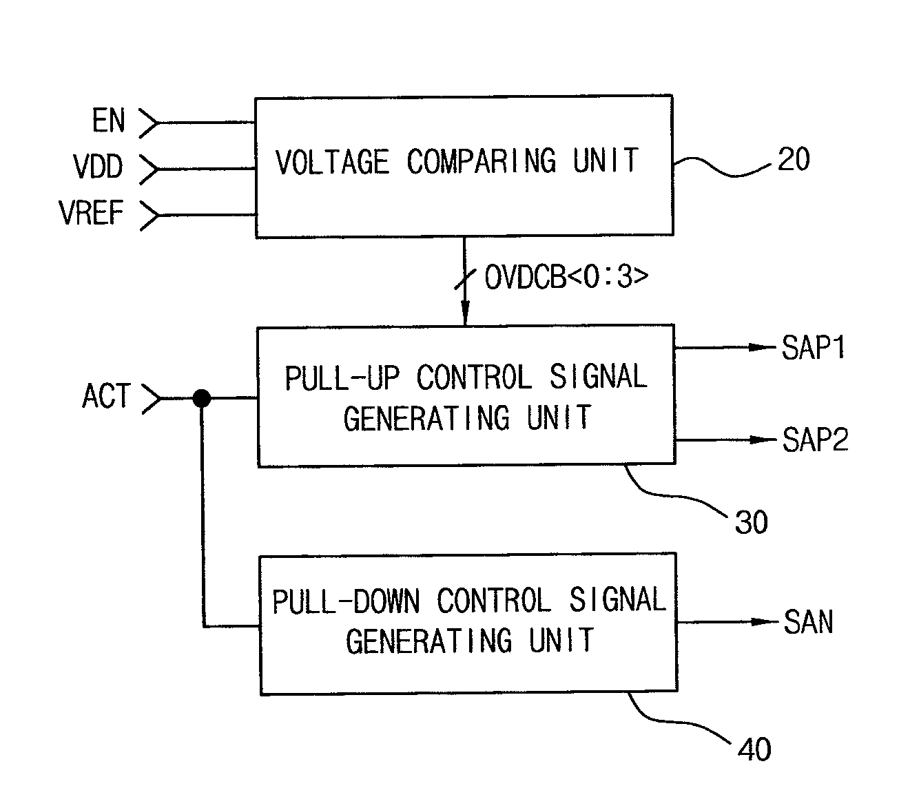
[0060]Referring to FIG. 5, the sense amplifier control circuit according to the present invention comprises a voltage comparing unit 20, a pull-up control signal generating unit 30, and a pull-down control generating unit 40.

[0061]The voltage comparing unit 20 outputs delay control signals OVDCB0:3> by comparing a divided voltage VD0 to VD3, obtained by dividing a power supply voltage VDD, with a reference voltage VREF when an enable signal EN is enabled.

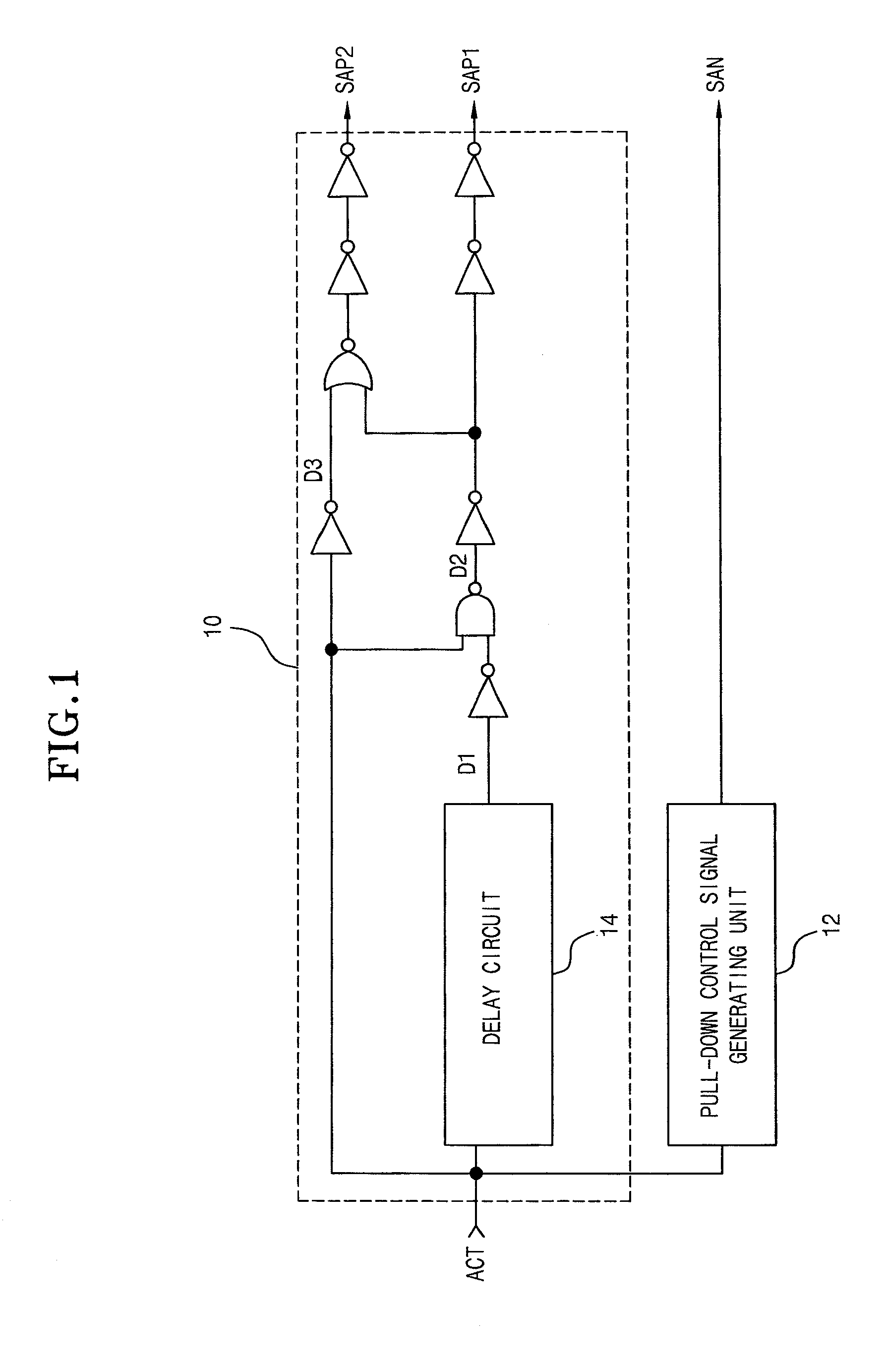
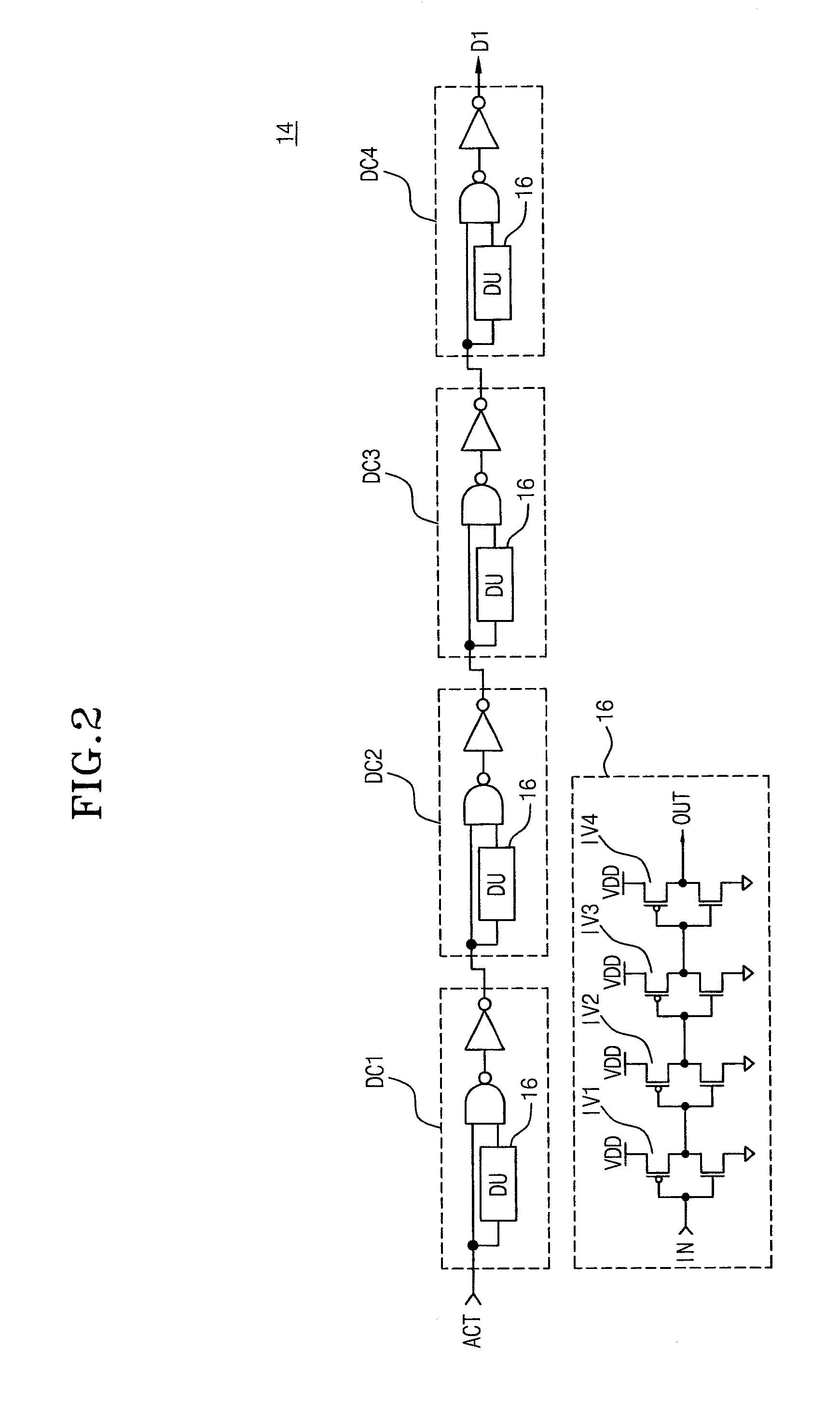
[0062]The pull-up control signal generating unit 30 outputs an overdrive control signal SAP1 and a pull-up control signal SAP2 of which an enable pulse width is controlled by a active signal ACT and the delay control signals OVDCB0:3>.

[0063]The pull-down control signal generating unit 40 outputs a pull-down control signal SAN which is enabled in synchronization with the overdrive control signal SAP1 in response to the active signal ACT.

[0064]Referring to FIG. 6, the voltage comparing unit 20 comprises a voltage dividing unit 22 that...

second embodiment

[0100]Referring to FIG. 10, the sense amplifier control circuit according to the present invention comprises a delay control signal generating unit 70, a path selecting unit 72, a delay control unit 74, a control signal generating unit 76, and a pull-down control signal generating unit 78.

[0101]The delay control signal generating unit 70 can be structured as the voltage comparing unit of FIG. 6. The delay control signal generating unit 70 compares the reference voltage VREF with the divided voltages obtained by dividing the power supply voltage VDD by utilizing a plurality of resistors in series, and the delay control signal generating unit 70 provides the delay control signal OVDCB in accordance with the comparing results when the enable signal EN is enabled,

[0102]More specifically, the delay control signal generating unit 70 disables all of the delay control signals OVDCB0:3> at a high level to output them if the potentials of the divided voltages VD0 to VD3 are higher than that o...


PUM


Abstract

The present invention discloses a sense amplifier control circuit which controls the sense amplifier. A sense amplifier control circuit comprises a voltage comparing unit outputting delay control signals having a value corresponding to each of divided voltages obtained by dividing a potential of a power supply voltage and a pull-up control signal generating unit outputting an overdrive control signal and a pull-up control signal by an active signal and changing an enable pulse width of the overdrive control signal in response to the delay control signals, whereby it is possible to reduce current consumption caused by unnecessary overdrive operation and prevent a potential drop of the power supply voltage and thus provide operational stability of the semiconductor memory device by providing the overdrive control signal of which the enable pulse width is controlled in response to the potential of the power supply voltage.

Description

CROSS-REFERENCE TO RELATED APPLICATIONS[0001]The present application claims priority to Korean patent application number 10-2007-0102812 filed on Oct. 11, 2007, which is incorporated herein by reference in its entirety.BACKGROUND OF THE INVENTION[0002]The present invention relates generally to a semiconductor memory device, and more precisely to a sense amplifier control circuit controlling a sense amplifier.[0003]In general, a semiconductor memory device includes the sense amplifier, which senses and amplifies the charge sharing in bit line of the semiconductor memory device by an active signal. In order to improve the amplifying speed of the sense amplifier, the memory device can use an overdriving method that drives the sense amplifier with an overdrive voltage, e.g., a boost voltage VPP, higher than a core voltage VCORE which is a cell capacitance potential at the beginning of amplification. Referring to FIG. 1, the sense amplifier control circuit comprises a pull-up control sig...

Claims


Application Information

Patent Timeline
IPC IPC(8): G11C7/08
CPCG11C7/08G11C5/145G11C7/22G11C2207/065
Inventor CHI, SUNG SOO
Owner SK HYNIX INC
Why Eureka
Try Eureka