Light-Emitting Element, Light-Emitting Device, and Electronic Device

a technology of light-emitting elements and light-emitting devices, which is applied in the direction of organic semiconductor devices, discharge tubes/lamp details, discharge tubes luminescnet screens, etc., can solve the problems of inability to easily achieve, short lifetime of light-emitting elements, and low durability of hole-blocking layers, so as to reduce the amount of injection of holes, increase the luminous efficiency of light-emitting elements, and reduce the effect of injection

Active Publication Date: 2009-04-23
SEMICON ENERGY LAB CO LTD
View PDF64 Cites 53 Cited by
  • Summary
  • Abstract
  • Description
  • Claims
  • Application Information

AI Technical Summary

Benefits of technology

[0020]The present invention makes it possible to suppress the injection amount of holes which are carriers of the light-emitting element, from the first layer (the hole-injecting layer) into the second layer (the hole-transporting layer); thus, recombination probability within the light-emitting layer can be increased and luminous efficiency of the light-emitting element can be increased. Moreover, b

Problems solved by technology

This cannot be easily achieved with a point light source typified by an incandescent lamp or an LED, or with a line light source typified by a fluorescent lamp.
There are many problems which depend on substances in improving element cha

Method used


Image

  • Light-Emitting Element, Light-Emitting Device, and Electronic Device
  • Light-Emitting Element, Light-Emitting Device, and Electronic Device
  • Light-Emitting Element, Light-Emitting Device, and Electronic Device

Examples


embodiment mode 1

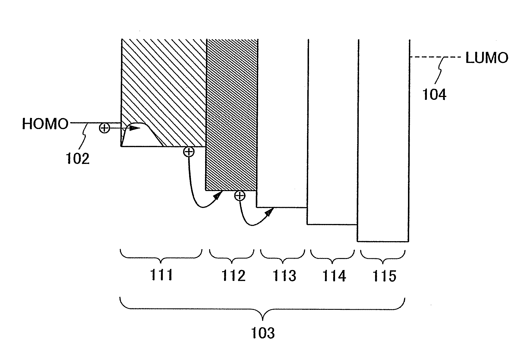
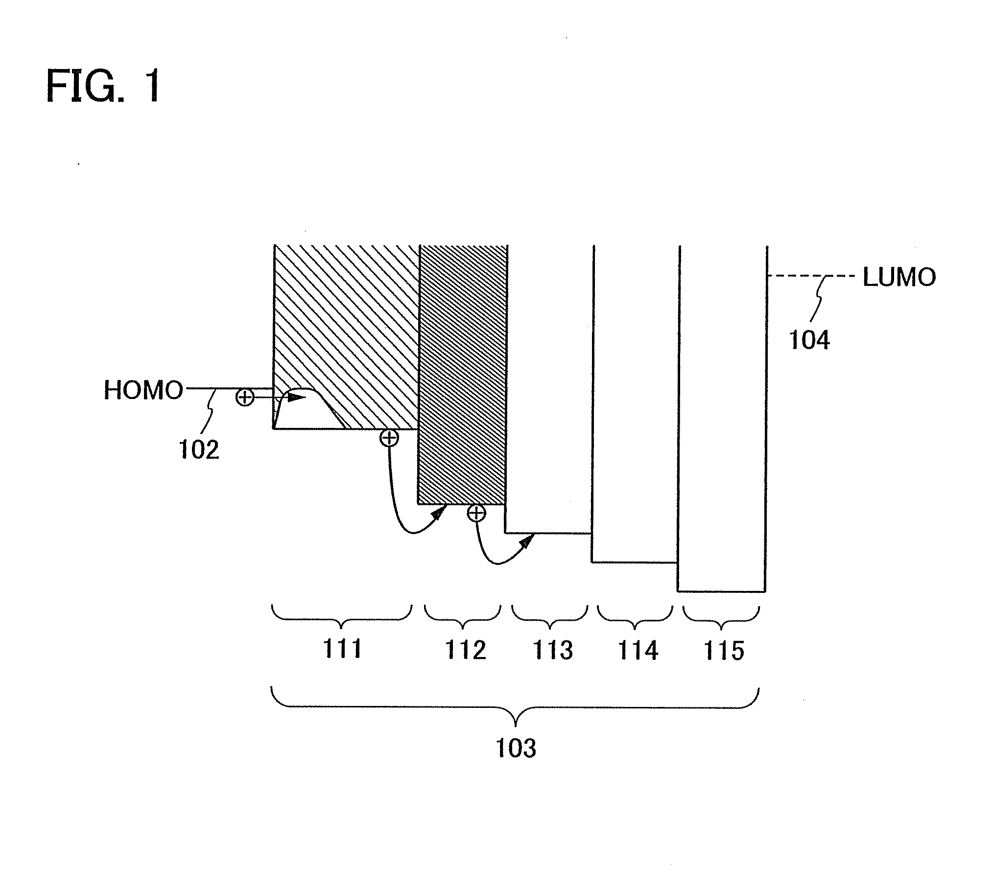
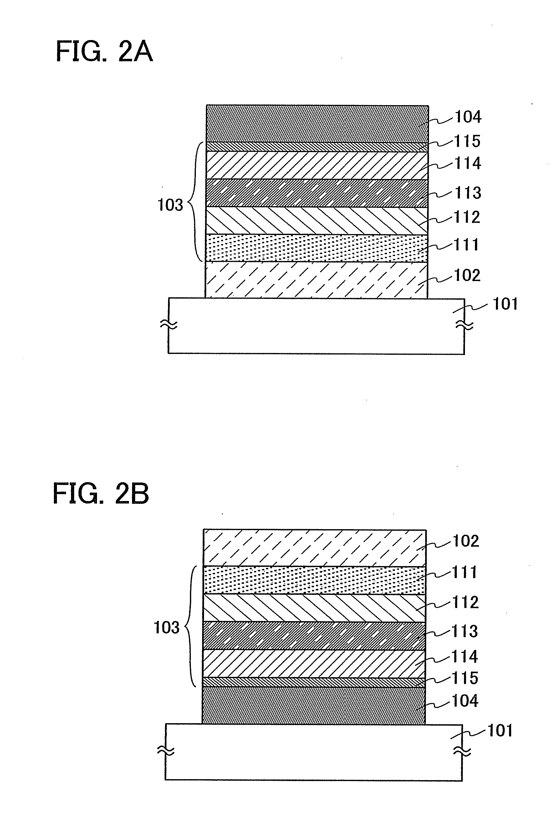
[0056]In Embodiment Mode 1, a light-emitting element of the present invention having a structure which is capable of suppressing the injection amount of holes from a first layer (a hole-injecting layer) into a second layer (a hole-transporting layer) of the light-emitting element will be described.

[0057]The light-emitting element in Embodiment Mode 1 includes a first electrode functioning as an anode, a second electrode functioning as a cathode, and an EL layer provided between the first electrode and the second electrode. As for the EL layer, it is acceptable as long as at least a hole-injecting layer, a hole-transporting layer, and a light-emitting layer are sequentially stacked from the first electrode side; the hole-injecting layer is formed of a composite material which makes it easy to inject holes regardless of the work function of the first electrode; and the hole-transporting layer and the hole-injecting layer are provided so that the HOMO level (the absolute value) of the ...

embodiment mode 2

[0113]In Embodiment Mode 2, a light-emitting element of the present invention which has a structure which reduces the electron transport rate in addition to the structure described in Embodiment Mode 1, which controls the injection amount of holes, will be described.

[0114]A light-emitting element in Embodiment Mode 2 includes a first electrode, a second electrode, and an EL layer provided between the first electrode and the second electrode. In the EL layer, at least a hole-injecting layer, a hole-transporting layer, a light-emitting layer, and a carrier-controlling layer are sequentially stacked from the first electrode side; and it is acceptable as long as the hole-injecting layer is formed of a composite material, and the hole-transporting layer and the hole-injecting layer are provided so that the HOMO level (the absolute value) of the hole-transporting layer becomes deeper (higher) than that of the hole-injecting layer. There is no particular limitation on other layers.

[0115]Th...

embodiment mode 3

[0174]In Embodiment Mode 3, a light-emitting element having a plurality of EL layers of the light-emitting elements described in Embodiment Modes 1 and 2 (hereinafter, such a light-emitting element is referred to as a “stacked-type light-emitting element”) will be described with reference to FIG. 8. This light-emitting element is a stacked-type light-emitting element which has a plurality of EL layers (a first EL layer 803 and a second EL layer 804) between a first electrode 801 and a second electrode 802. Note that, although a structure of two EL layers is described in Embodiment Mode 3, a structure of three or more EL layers may be employed.

[0175]In Embodiment Mode 3, the first electrode 801 functions as an anode and the second electrode 802 functions as a cathode. Note that the first electrode 801 and the second electrode 802 can be made to have structures similar to those described in Embodiment Mode 1. Further, for the plurality of EL layers (the first EL layer 803 and the seco...


PUM


Abstract

In a light-emitting element including an EL layer between a pair of electrodes, a structure is formed in which the EL layer includes at least a first layer having a hole-injecting property (a hole-injecting layer) and a second layer having a hole-transporting property (a hole-transporting layer) between the electrode functioning as an anode and a third layer having a light-emitting property (a light-emitting layer), and the absolute value of the highest occupied molecular orbital level (HOMO level) of the second layer is larger than that of the first layer, so that the injection amount of holes from the electrode side which functions as an anode is suppressed, and thus luminous efficiency of the light-emitting element is increased.

Description

TECHNICAL FIELD[0001]The present invention relates to a current excitation type light-emitting element in which a light-emitting substance is interposed between a pair of electrodes, a light-emitting device having such a light-emitting element, and an electronic device.BACKGROUND ART[0002]In recent years, research and development have been extensively conducted on light-emitting elements using electroluminescence. In a basic structure of such a light-emitting element, a layer containing a substance having a light-emitting property is interposed between a pair of electrodes. By application of voltage to this element, light emission from the substance having a light-emitting property can be obtained.[0003]Since such a light-emitting element is of self-luminous type, it has advantages over a liquid crystal display, such as high visibility of the pixels and no need of a backlight, and is considered to be suitable as a flat panel display element. In addition, such a light-emitting elemen...

Claims


Application Information

Patent Timeline
IPC IPC(8): H01J1/63
CPCH01L51/0059H01L51/006H01L51/0071H01L2251/552H01L51/5048H01L51/5052H01L51/5088H01L51/0072H10K85/633H10K85/631H10K85/657H10K85/6572H10K50/155H10K50/14H10K50/17H10K2101/30H10K2101/40
Inventor SHITAGAKI, SATOKOSUZUKI, TSUNENORISEO, SATOSHI
Owner SEMICON ENERGY LAB CO LTD
Why Eureka
Try Eureka