Method of magnetic tunneling layer processes for spin-transfer torque MRAM

a technology of magnetic tunneling layer and spin-transfer torque, which is applied in the manufacture/treatment of electrical equipment, semiconductor devices, and electrical devices of magnetic devices, etc., can solve the problems of stt-mram's fundamental limitation of scalability, the fabrication process of stt-mram is very challenging, and the aspect ratio (thickness/cd) may become too larg

Active Publication Date: 2009-04-23
TAIWAN SEMICON MFG CO LTD
View PDF10 Cites 42 Cited by
  • Summary
  • Abstract
  • Description
  • Claims
  • Application Information

AI Technical Summary

Benefits of technology

[0015]One objective of the present invention is to provide a process for fabricating a MTJ element for a STT-MRAM device that enables two dimensional (CD) control in easy-axis and hard-axis directions while printing a post pattern.

Problems solved by technology

However, conventional MRAM has a fundamental limitation of scalability.
The fabrication process of a STT-MRAM is very challenging because of the small MTJ size where both easy-axis and hard axis dimensions must be controlled for optimum performance.
If the resist thickness is increased to provide extra process latitude for a subsequent etch step, then the aspect ratio (thickness / CD) may become too large and the post could collapse during image development.
On the other hand, if the photoresist thickness is made thinner to allow smaller features to be printed with a larger process window without image collapse, then there may not be enough photoresist to serve as an adequate etch mask during a subsequent etch step where the photoresist pattern is transferred through the MTJ stack of layers.
However, the challenge is to apply existing photolithography techniques to MRAM MTJ fabrication.

Method used


Image

  • Method of magnetic tunneling layer processes for spin-transfer torque MRAM
  • Method of magnetic tunneling layer processes for spin-transfer torque MRAM
  • Method of magnetic tunneling layer processes for spin-transfer torque MRAM

Examples


first embodiment

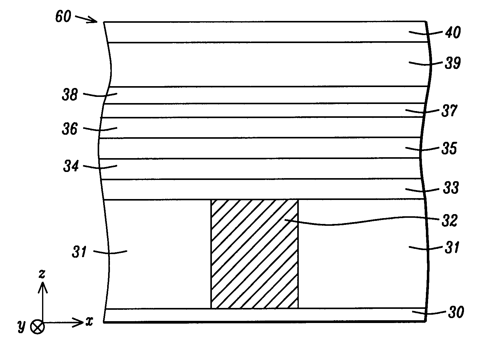
[0038]A method of forming a MTJ element in a STT-MRAM structure according to the present invention will now be described. Referring to FIG. 5, a partially completed STT-MRAM structure 60 is shown that includes a substrate 30 which may be a CMOS substructure used in the art that typically contains devices such as transistors and diodes. A first insulation layer 31 comprised of Al2O3, silicon oxide, or the like is disposed on the substrate 30. There is a metal contact 32 to the CMOS substructure 31 formed within and coplanar with the first insulation layer 31. The metal contact 32 may be made of copper, for example. It should be understood that there is a plurality of metal contacts 32 formed within the first insulation layer 31, and there is a plurality of STT-MRAMs 60 formed on the substrate 30. However, only one metal contact and one STT-MRAM are depicted to simplify the drawing. There is also a plurality of bit lines and word lines (not shown) formed in a cross-point architecture ...

second embodiment

[0065]To summarize the second embodiment, the combination of the two photolithography steps and two etch steps that determine the CDs along the easy-axis and hard-axis directions may result in at least four configurations represented by FIGS. 15a-15b and FIGS. 16a-16b. In one aspect, the first etch and second etch may both stop on the bottom electrode layer 33. In a second configuration, the first etch and second etch may both stop on the tunnel barrier layer 37 or inside the free layer 38. In a third configuration, one etch may stop on the bottom electrode and the other etch may stop on the tunnel barrier layer (or inside the free layer). Thus, FIG. 15b may represent a view from the plane 51-51 that includes the hard axis and FIG. 16b may represent a view from the plane 50-50 that includes the easy-axis. The present invention also anticipates that the plane 50-50 may include the hard-axis and plane 51-51 may include the easy-axis.

[0066]Subsequent process steps to complete the STT-M...


PUM


Abstract

A method for forming a MTJ in a STT-MRAM is disclosed in which the easy-axis CD is determined independently of the hard-axis CD. One approach involves two photolithography steps and two etch steps to form a post in a hard mask which is transferred through a MTJ stack of layers by a third etch process. Optionally, the third etch may stop on the tunnel barrier or in the free layer. A second embodiment involves forming a first parallel line pattern on a hard mask layer and transferring the line pattern through the MTJ stack with a first etch step. A planar insulation layer is formed adjacent to the sidewalls in the line pattern and then a second parallel line pattern is formed which is transferred by a second etch through the MTJ stack to form a post pattern. Etch end point may be controlled independently for hard-axis and easy-axis dimensions.

Description

RELATED PATENT APPLICATION[0001]This application is related to the following: Docket # HMG06-042 / 051, Ser. No. 11 / 699,875, filing date Jan. 30, 2007; assigned to a common assignee and herein incorporated by reference in its entirety.FIELD OF THE INVENTION[0002]The invention relates to a method of fabricating a magnetic tunneling junction (MTJ) element for improved critical dimension (CD) control along easy-axis and hard-axis directions and flexible etch end point which provides improved performance in spin-transfer torque MRAM (STT-MRAM) devices.BACKGROUND OF THE INVENTION[0003]Magnetoresistive Random Access Memory (MRAM), based on the integration of silicon based Complementary Silicon-Oxide Semiconductor (CMOS) with MTJ technology, is a technology that is highly competitive with existing semiconductor memories such as SRAM, DRAM, Flash, etc. MRAM is now a proven nonvolatile memory technology with many advantages over other commercialized memory types in terms of writing / read speed,...

Claims


Application Information

Patent Timeline
Patent Type & Authority Applications(United States)
IPC IPC(8): H01L21/00
CPCB82Y10/00H01L43/12H01L27/228H10B61/22H10N50/01
Inventor ZHONG, TOMXIAO, RONGFUTORNG, CHYU-JIUHZHONG, ADAM
Owner TAIWAN SEMICON MFG CO LTD
Why Eureka
Try Eureka