Optical element, liquid crystal device, and electronic apparatus

Inactive Publication Date: 2009-04-30
SEIKO EPSON CORP
View PDF19 Cites 46 Cited by
  • Summary
  • Abstract
  • Description
  • Claims
  • Application Information

AI Technical Summary

Benefits of technology

[0017]An advantage of the invention is to provide an optical element having a wire grid polarization layer easily manufactured and superior optical characteristics, a liquid crystal device having high functions and manufactured by simplified processes, and an electronic apparatus.
[0018]According to a first aspect of the invention, an optical element includes: a substrate; a grid formed on the substrate, the grid including a plurality of micro-wires and having a polarization-separation function; and a diffraction function layer formed above the grid. In the element, the diffraction function layer has at least two kinds of regions in a plane, and at least the two kinds of regions have different refractive indexes.
[0019]The optical element has the grid on the plane of the substrate. This structure can improve the uniformity of an exposure amount of a resis

Problems solved by technology

This results in the luminance in a viewing direction being lowered, making difficult to see images.
As a result, the resist film 513 cannot be formed with a uniform thickness.
As a result, a resist pattern having a uniform shape cannot be achieved.
This structure also has a problem from a point of view of the performance of a liquid crystal device.
This variation cause

Method used


Image

  • Optical element, liquid crystal device, and electronic apparatus
  • Optical element, liquid crystal device, and electronic apparatus
  • Optical element, liquid crystal device, and electronic apparatus

Examples


Embodiment Construction

[0077]Embodiments of the invention will be described below with reference to the drawings. Note that scales of members in the drawings referred to hereinafter are adequately changed so that they can be recognized.

[0078]Optical Element

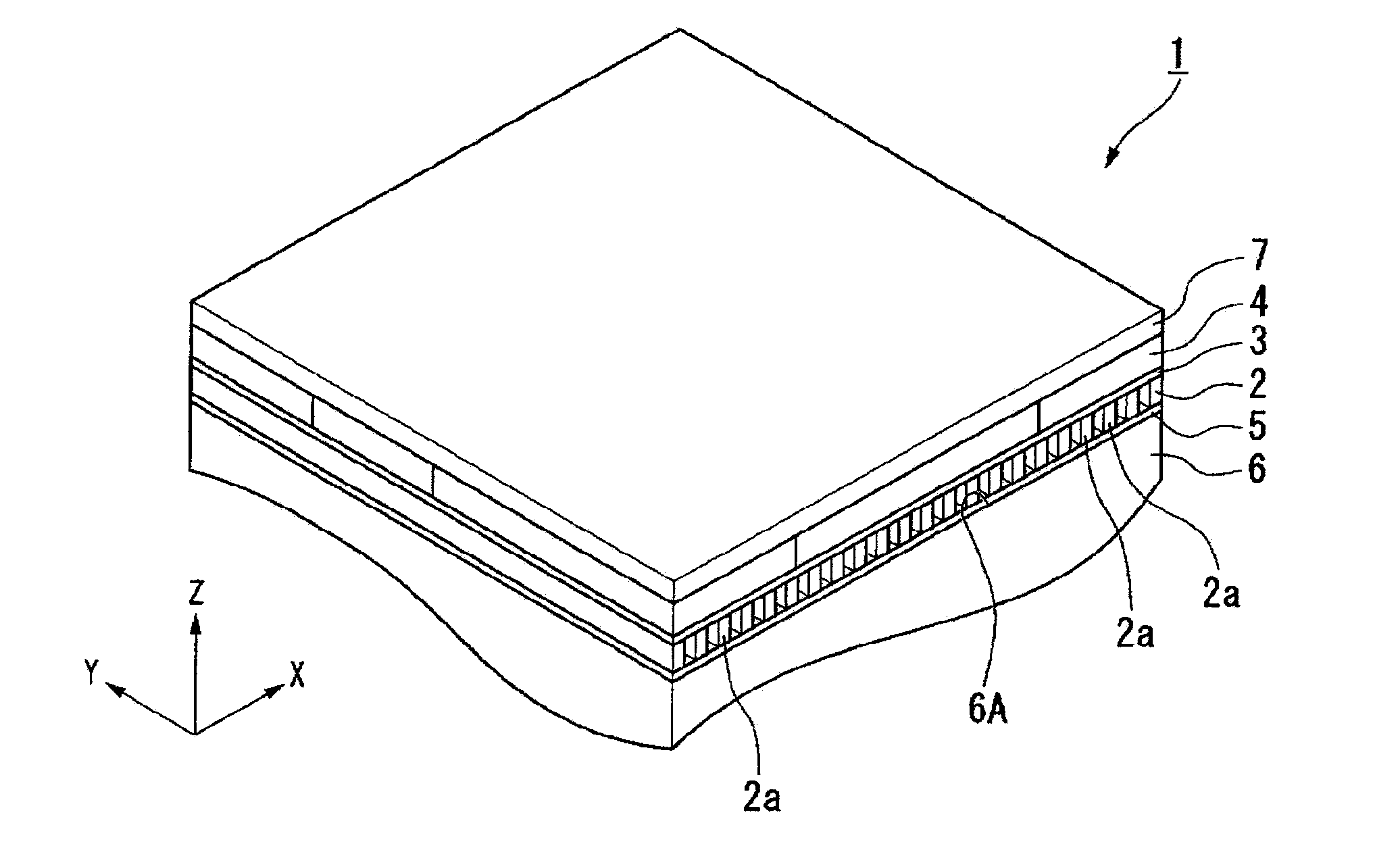
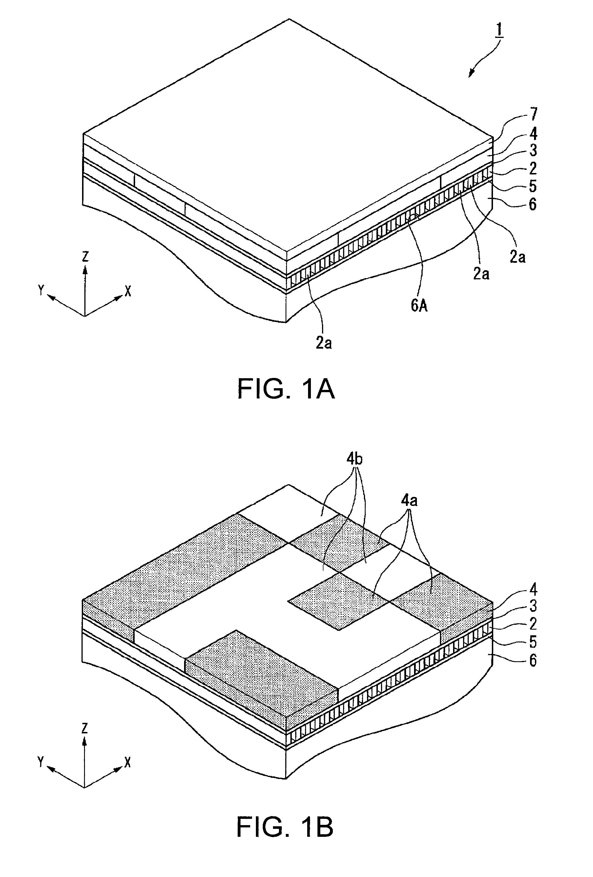
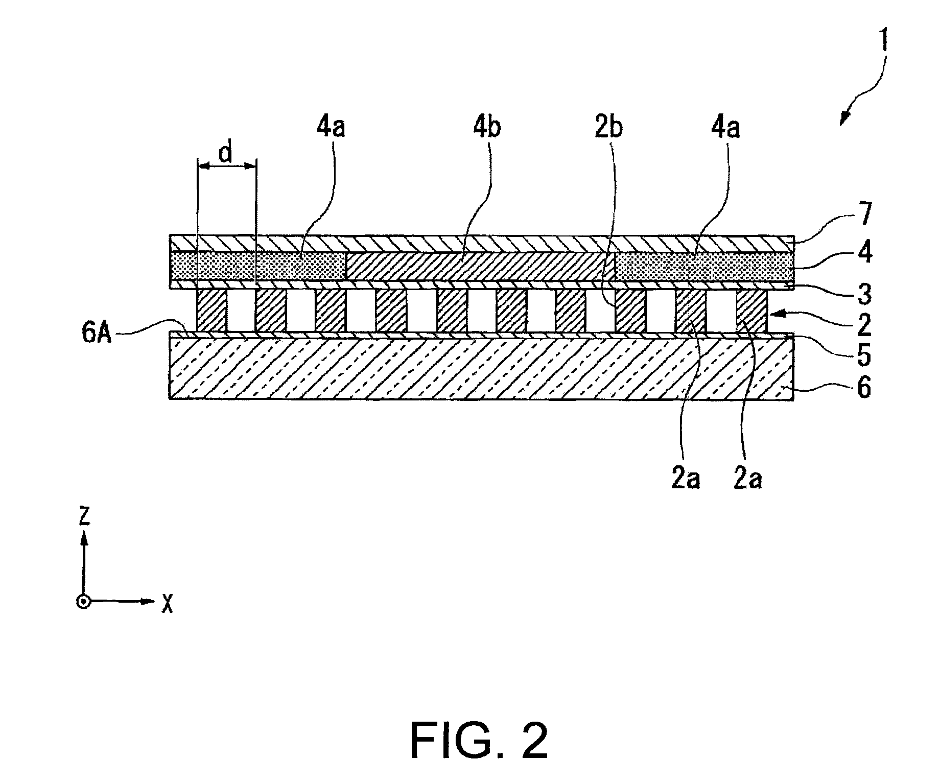
[0079]FIGS. 1A and 1B are perspective views schematically showing the structure of an optical element according to an embodiment of the invention. FIG. 2A is a sectional view of an optical element 1 taken along the X-Z plane in FIG. 1A. The optical element 1 includes a substrate 6, a wire grid polarization layer 2 disposed on the substrate 6, a diffraction function layer 4 disposed above the wire grid polarization layer 2 with a covering layer 3 interposed therebetween, an AR coat film 7, and a counter substrate (not shown).

[0080]FIG. 1B is a perspective view showing the arrangement of the diffraction function layer.

[0081]The substrate 6 is a transparent substrate such as glass, quartz, and plastic. As shown in FIG. 2, the wire grid polarization layer 2...


PUM


Abstract

An optical element includes: a substrate; a grid formed on the substrate, the grid including a plurality of micro-wires and having a polarization-separation function; and a diffraction function layer formed above the grid. In the element, the diffraction function layer has at least two kinds of regions in a plane, and at least the two kinds of regions have different refractive indexes.

Description

BACKGROUND[0001]The entire disclosure of Japanese Patent Application No. 2007-283169, filed Oct. 31, 2007 is expressly incorporated by reference herein.[0002]1. Technical Field[0003]The present invention relates to an optical element, a liquid crystal device and an electronic apparatus.[0004]2. Related Art[0005]A wire grid polarization element is known as one of optical elements having a polarization-separation function. The element has a number of conductive micro-wires arranged at a pitch smaller than the wavelength of light. The element also has the property of reflecting a component (TE) having a polarization axis parallel to the micro-wires and transmitting a component (TM) having a polarization axis perpendicular to the micro-wires among components of incident light.[0006]When such wire grid polarization element is built in a semi-transmissive-reflective liquid crystal device, a wire grid polarization layer and a scattering layer are layered to a region corresponding to a refl...

Claims


Application Information

Patent Timeline
IPC IPC(8): G02F1/1335G02B5/30
CPCG02B5/1814G02B5/3058G02F2001/133548G02F1/133528G02F1/133504G02F1/133548
Inventor SAWAKI, DAISUKEKENMOCHI, NOBUHIKO
Owner SEIKO EPSON CORP
Why Eureka
Try Eureka