Method for power semiconductor module fabrication, its apparatus, power semiconductor module and its junction method

a technology of power semiconductor modules and fabrication methods, which is applied in the direction of semiconductor devices, semiconductor/solid-state device details, cooling/ventilation/heating modifications, etc., can solve the problems of increasing contact thermal resistance, achieve improved reliability, reduce the weight bearing of the first joining material, and reduce the contact thermal resistance

Inactive Publication Date: 2009-05-07
HITACHI LTD
View PDF4 Cites 67 Cited by
  • Summary
  • Abstract
  • Description
  • Claims
  • Application Information

AI Technical Summary

Benefits of technology

[0006]The present invention has been made in view of the above problem and it is an object of the present invention to provide a fabrication method of a power semiconductor module, a fabrication apparatus of a power semiconductor module, a power semiconductor module and a joining method in which contact thermal resistance is reduced and reliability is improved.
[0007]In order to achieve the above object, according to the present invention, the fabrication method of the power semiconductor module including first and second insulating substrates, a power semiconductor device joined directly or through another element to opposite sides of the first and second insulating substrates and first and second heat spreaders joined with ...

Problems solved by technology

Accordingly, there is a problem tha...

Method used


Image

  • Method for power semiconductor module fabrication, its apparatus, power semiconductor module and its junction method
  • Method for power semiconductor module fabrication, its apparatus, power semiconductor module and its junction method
  • Method for power semiconductor module fabrication, its apparatus, power semiconductor module and its junction method

Examples


first embodiment

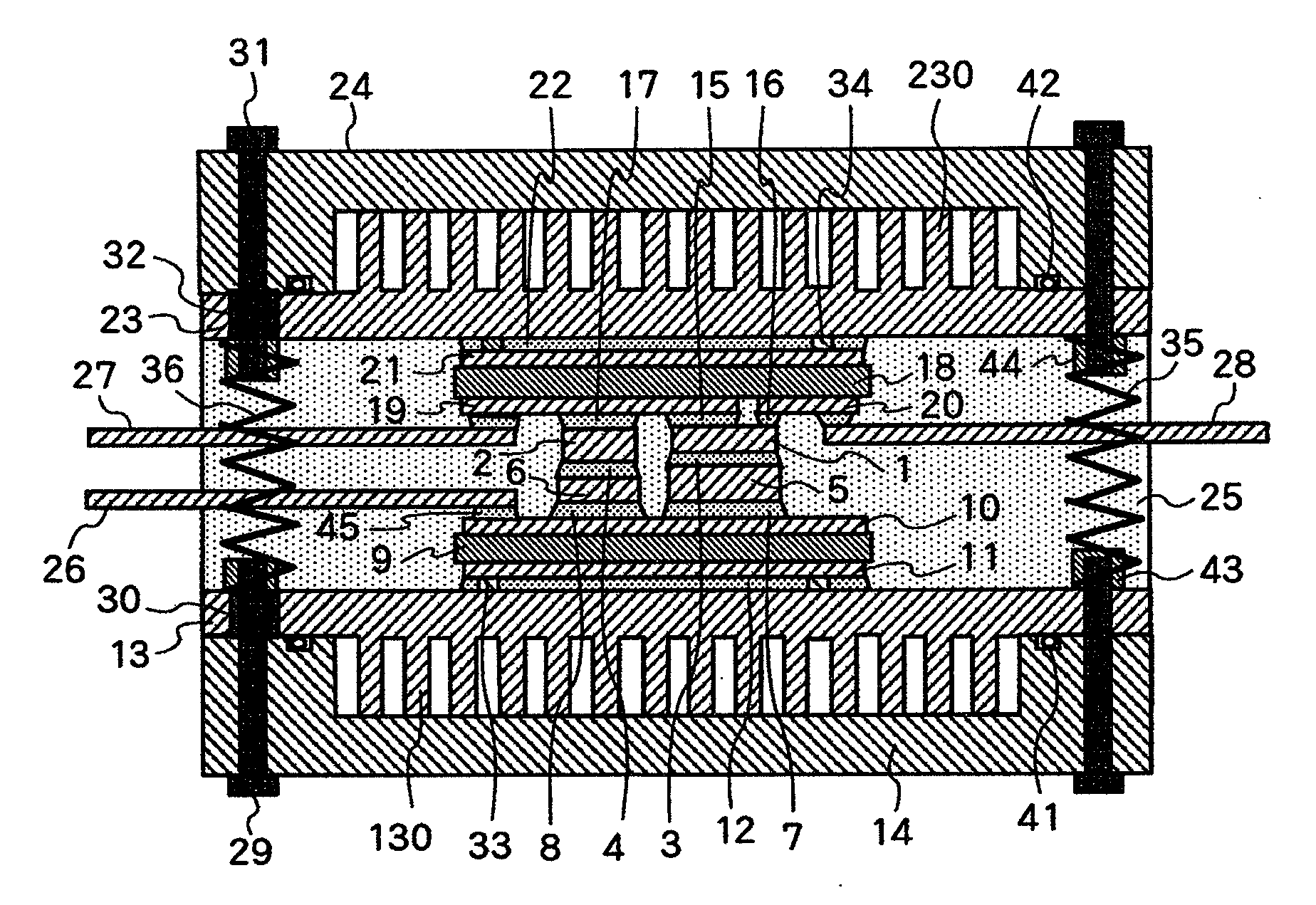
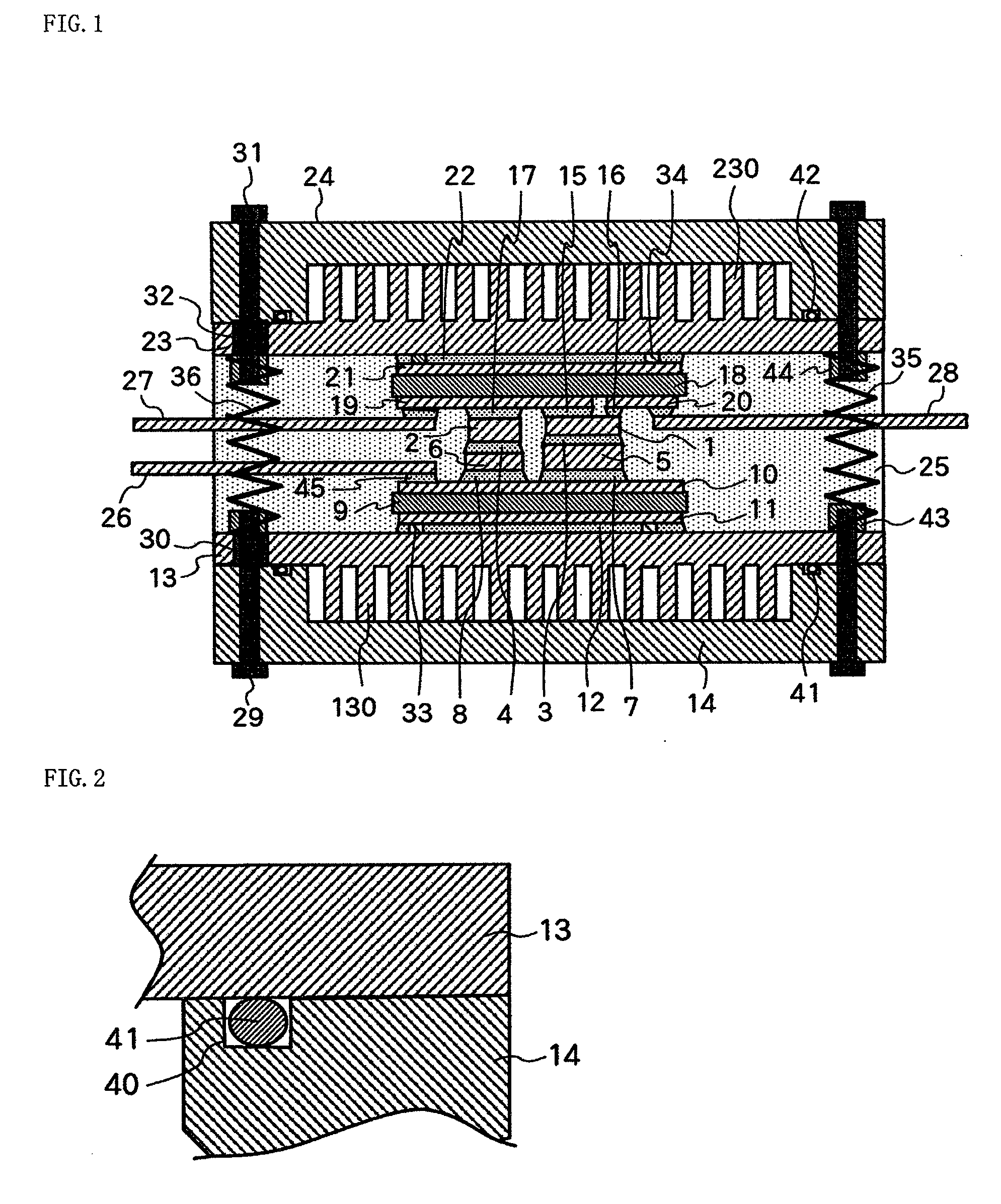
[0022]FIG. 1 is a sectional view illustrating a power semiconductor module according to an embodiment (first embodiment) of the present invention. Referring now to FIG. 1, elements constituting the power semiconductor module according to the embodiment are described.

[0023]Numerals 1 and 2 shown in FIG. 1 represent power semiconductor devices such as insulated gate bipolar transistors (IGBT) and free-wheel diodes.

[0024]Spacers 5 and 6 are connected or joined to the lower sides of the power semiconductor modules 1, 2 with joining materials 3 and 4 such as solder. The spacers 5, 6 have not only the function of adjusting height when the power semiconductor devices 1 and 2 are different in thickness thereof but also the function of preventing discharge from occurring between the electrodes 26 and 27 disposed over and under the devices since the distance therebetween is too short. The spacers 5, 6 are desired to have small electrical resistance and thermal resistance and may be made of no...

second embodiment

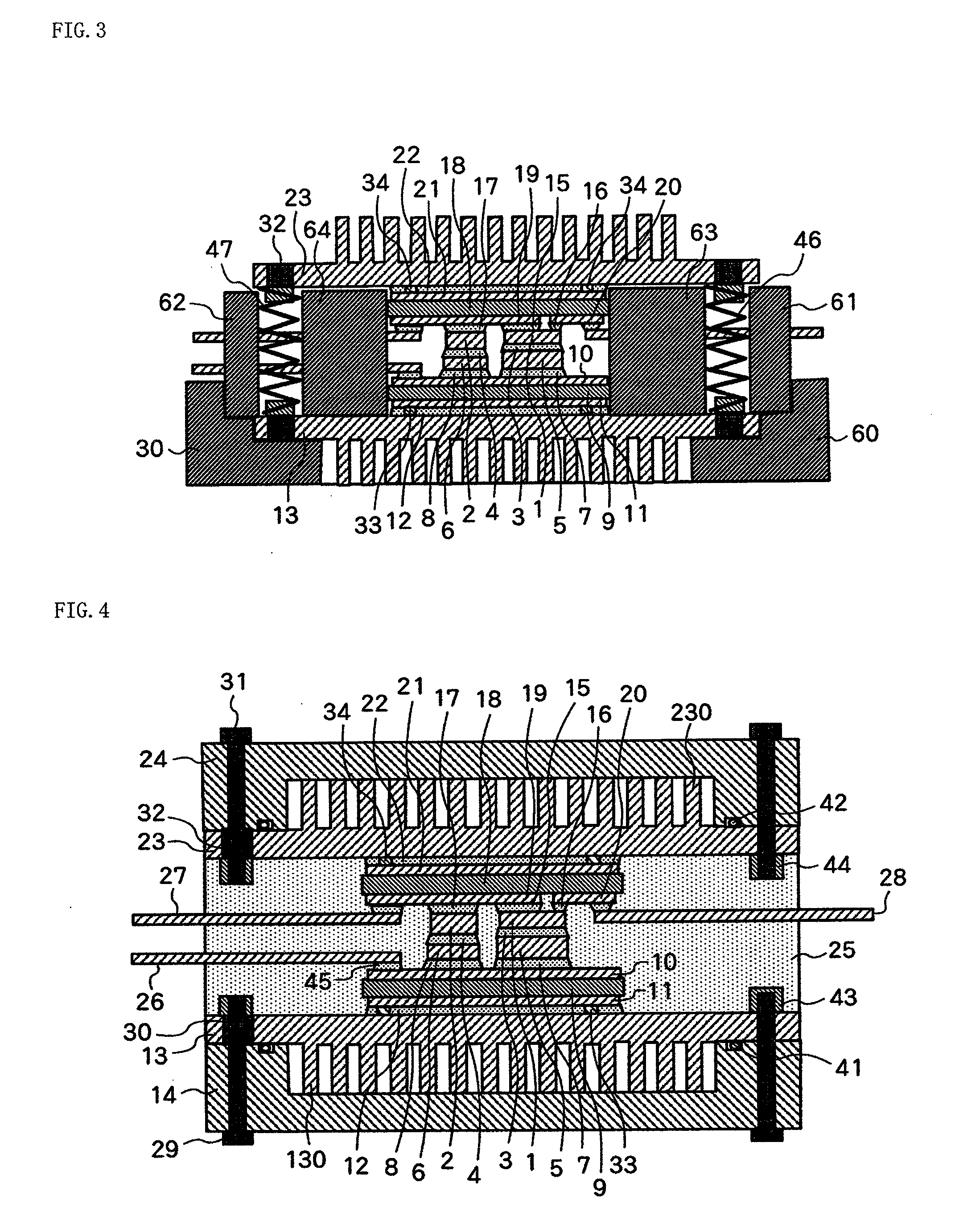
[0039]FIG. 7 is a sectional view illustrating a power semiconductor module and assembly jigs according to another embodiment (second embodiment) of the present invention. In the embodiment, when lower insulating substrate 9 and lower heat spreader 13 are joined to each other with joining material 12 and when upper insulating substrate 18 and upper heat spreader 23 are joined to each other with joining material 22, upper heat spreader 23 is hung from above by springs 48, 49. Springs 48 and 49 are supported by jigs 72 and 73, respectively. Springs 48, 49 may be metallic coil springs or plate springs. Alternatively, resin material having resilience may be used instead of metal. Upper heat spreader 23 is supported in this manner, so that the whole weight of heat spreader 23 does not directly bear on joining materials 12, 22 and accordingly joining materials such as solder can be prevented from being forced out of insulating substrate so as not to cause short-circuiting.

third embodiment

[0040]FIG. 8 is a sectional view illustrating a power semiconductor module and assembly jigs according to still another embodiment (third embodiment) of the present invention. In the embodiment, when power semiconductor devices 1, 2 and upper and lower insulating substrates 18, 9 are joined with joining material 7, 8, 15, 16 and 17, jigs 81 to 92 are used to hang the upper insulating substrate 18 by springs 37, 38. Jigs 89, 90 are attached to lower sides of springs, so that upper insulating substrate 18 is supported from bottom thereof by means of jigs 89, 90. Upper sides of springs 37, 38 are supported by jigs 87, 88. Jigs 87, 88 are fixed to jig 92. Thus, since the whole weight of upper insulating substrate and the like does not directly bear on joining materials, joining materials can be prevented from being forced out so as not to cause short-circuiting.

[0041]FIG. 9 is a sectional view illustrating a power semiconductor module according to a still further embodiment (fourth embo...


PUM


Abstract

A power semiconductor module includes first and second insulating substrates, a power semiconductor device joined directly or through another element to opposite sides of the first and second insulating substrates and first and second heat spreaders joined with joining material having fluidity upon joining so as to put the first and second insulating substrates between the first and second heat spreaders. When the power semiconductor module is fabricated, the first and second insulating substrates are joined to the first and second heat spreaders, respectively, in the state that weight bearing on joining material is reduced by means of resilient member.

Description

BACKGROUND OF THE INVENTION[0001]The present invention relates to a fabrication method of a power semiconductor module, a fabrication apparatus of a power semiconductor module, a power semiconductor module and a joining method.[0002]In recent years, a demand for increased output of an inverter used in a hybrid automobile is being increased and high output power of a power module constituting the inverter is required. On the other hand, there is restriction on space for installing components in an automobile and accordingly the power module is also required to be made more compact at the same time. Thus, in order to cope with the high output power and the compactness of the automobile, it is necessary to enhance cooling performance of the power module.[0003]Heretofore, JP-A-2005-175130 discloses, as technique for enhancing cooling performance of the power module, that electrodes, insulating sheets, heat spreaders and heat sinks are disposed over and under power semiconductor device t...

Claims


Application Information

Patent Timeline
IPC IPC(8): H01L23/34H01L21/58
CPCH01L21/4882H01L2924/13055H01L23/3735H01L23/4334H01L25/0655H01L25/072H01L2023/4081H01L2224/48091H01L2224/48247H01L2224/73215H01L2224/73265H01L23/367H01L2924/1305H01L24/48H01L2224/32225H01L2924/00014H01L2924/00H01L2224/33H01L2224/2612H01L2224/45099H01L2224/45015H01L2924/207
Inventor FUNAKOSHI, SUNAOISHIKAWA, KATSUMISOGA, TASAO
Owner HITACHI LTD
Why Eureka
Try Eureka