Spin field effect transistor using half metal and method of manufacturing the same

a technology of spin field and transistor, which is applied in the direction of magnetic materials, magnetic bodies, nanomagnetism, etc., can solve the problems of increasing the power requirement may not be reduced, and the rate of carrier mobility may not keep increasing

Active Publication Date: 2009-05-14
SAMSUNG ELECTRONICS CO LTD
View PDF3 Cites 16 Cited by
  • Summary
  • Abstract
  • Description
  • Claims
  • Application Information

AI Technical Summary

Benefits of technology

[0053]The spin field effect transistor that uses a half metal according to example embodiments may have increased charge mobility as compared to a conventional semiconductor device. Also, in the spin field effect transistor, the power needed to change the direction of the electron spin may be smaller than the power required to change the electrons. Thus, the amount of power required for the operation may be reduced. Accordingly, a relatively small spin field effect transistor may be manufactured through a scale down.

Problems solved by technology

When semiconductor devices are manufactured to a nanoscale, the increasing rate of carrier mobility may not keep pace with the increasing rate of the semiconductor devices, and despite the reduction in the size of devices, the power requirement may not be reduced.

Method used


Image

  • Spin field effect transistor using half metal and method of manufacturing the same
  • Spin field effect transistor using half metal and method of manufacturing the same
  • Spin field effect transistor using half metal and method of manufacturing the same

Examples


Embodiment Construction

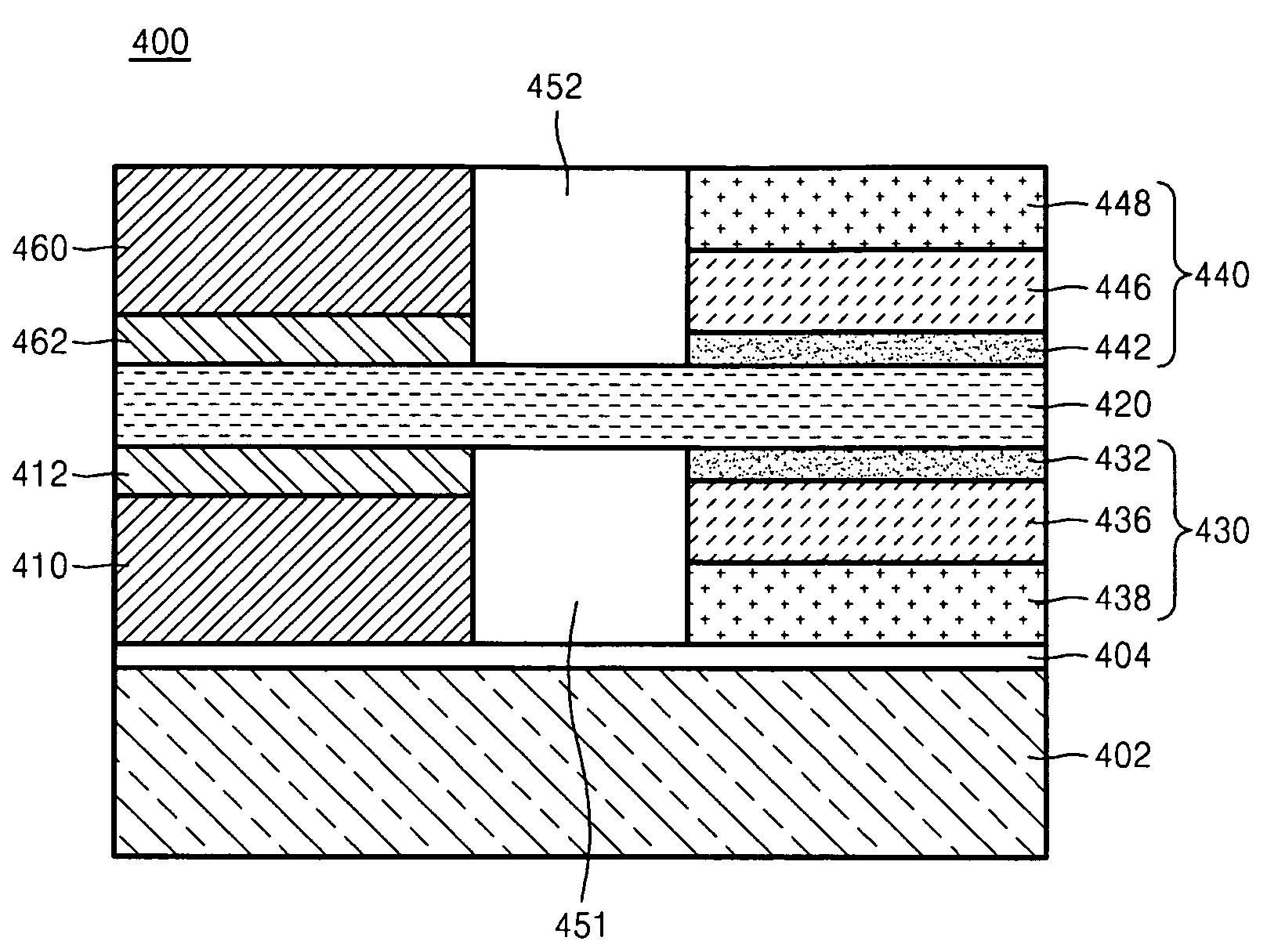
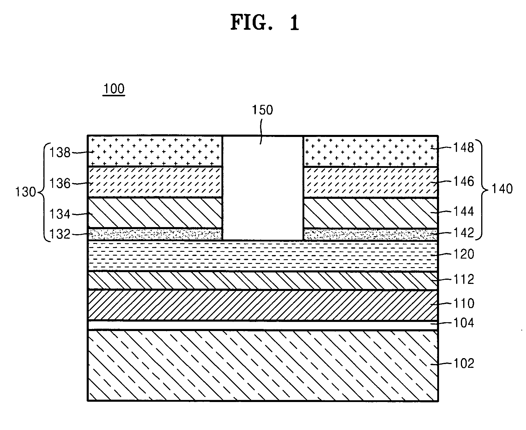
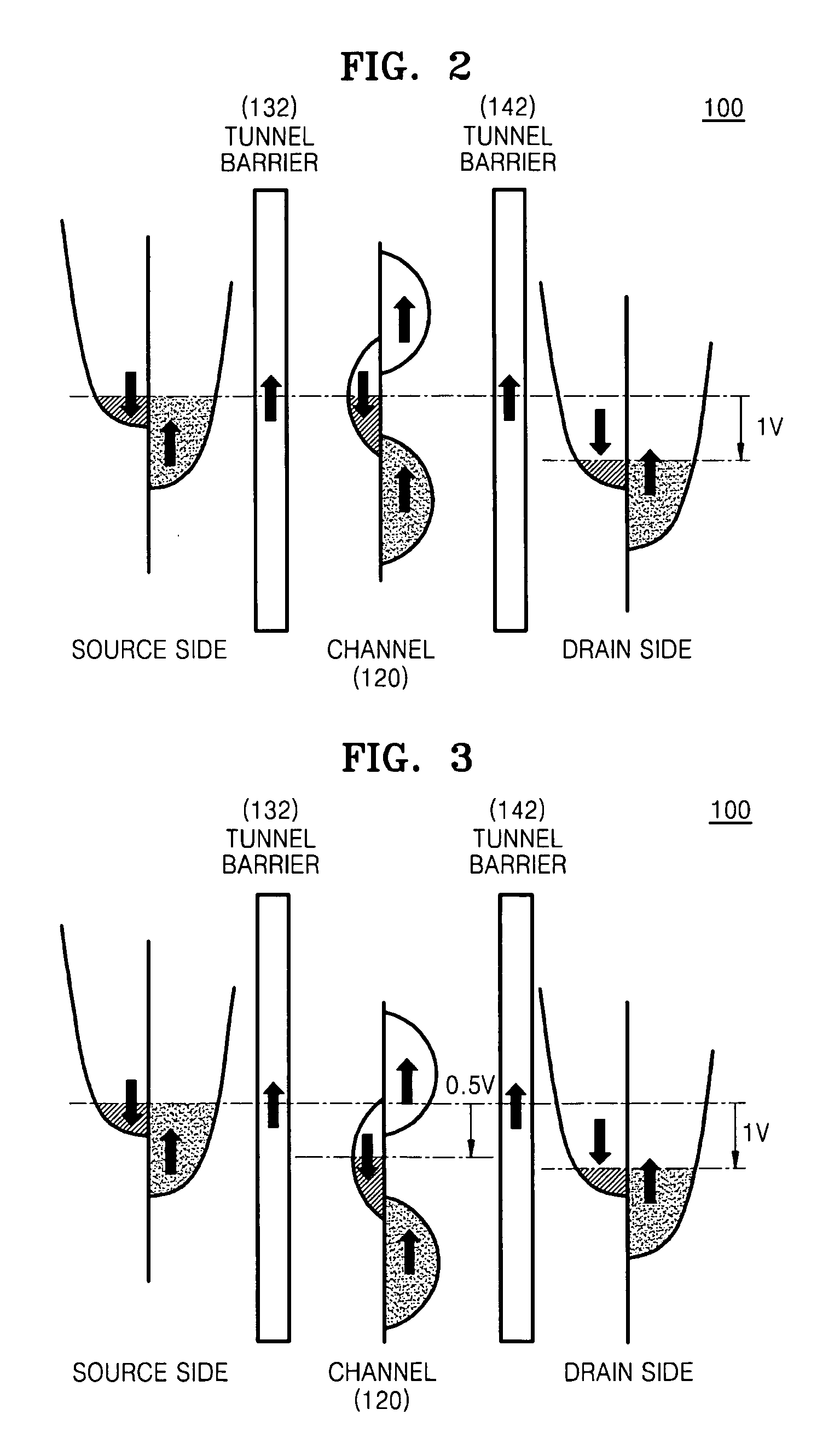
[0026]Example embodiments will now be described more fully with reference to the accompanying drawings in which example embodiments may be shown. In the drawings, the thicknesses of layers and regions may be exaggerated for clarity. Like reference numerals denote like elements in the drawings and repetitive description thereof will be omitted.

[0027]It will be understood that when an element is referred to as being “connected” or “coupled” to another element, it can be directly connected or coupled to the other element or intervening elements may be present. In contrast, when an element is referred to as being “directly connected” or “directly coupled” to another element, there are no intervening elements present. Like numbers indicate like elements throughout. As used herein the term “and / or” includes any and all combinations of one or more of the associated listed items.

[0028]It will be understood that, although the terms “first”, “second”, etc. may be used herein to describe vario...


PUM

PropertyMeasurementUnit
ground voltageaaaaaaaaaa
gate voltageaaaaaaaaaa
chemical compositionaaaaaaaaaa

Abstract

A spin field effect transistor may include at least one gate electrode, a channel layer, a first stack and a second stack separate from each other on a substrate, wherein the channel layer is formed of a half metal. The half metal may be at least one material selected from the group consisting of chrome oxide (CrO2), magnetite (Fe3O4), a double perovskite structure material, a Heusler alloy, NiMnSb, La(1-x)AxMnO3 (A=Ca, Ba, Sr, x˜0.3), and GaN doped with Cu, and the double perovskite structure material is expressed as a chemical composition of A2BB′O6, and a material corresponding to A is Ca, Sr, or Ba, a material corresponding to B is a 3d orbital transition metal, and a material corresponding to B′ is a 4d orbital transition metal. The 3d orbital transition metal may be Fe or Co, and the 4d orbital transition metal is Mo or Re.

Description

PRIORITY STATEMENT[0001]This application claims priority under U.S.C. §119 to Korean Patent Application No. 10-2007-0114192, filed on Nov. 9, 2007, in the Korean Intellectual Property Office (KIPO), the entire contents of which are incorporated herein by reference.BACKGROUND[0002]1. Field[0003]Example embodiments relate to a spin field effect transistor that uses a half metal as a channel and a method of manufacturing the same.[0004]2. Description of the Related Art[0005]When semiconductor devices are manufactured to a nanoscale, the increasing rate of carrier mobility may not keep pace with the increasing rate of the semiconductor devices, and despite the reduction in the size of devices, the power requirement may not be reduced. In order to address these problems, a technique of using electron spin has been proposed.[0006]As such, a spin field effect transistor may be turned on using the spin of electrons, and the power required for electron spinning may be smaller and the turn on...

Claims


Application Information

Patent Timeline
Patent Type & Authority Applications(United States)
IPC IPC(8): H01L29/82
CPCH01L29/66984H01L29/82H01F1/404H01F10/3254H01F10/1933H01F10/3295B82Y25/00H01F1/401H01F10/1936
Inventor HONG, KI-HALEE, SUNG-HOONKIM, JONG-SEOBSHIN, JAI KWANG
Owner SAMSUNG ELECTRONICS CO LTD
Why Eureka
Try Eureka