[0010]In Equation 1, Ids denotes the
drain current that flows between the source and the drain. This current is equivalent to the output current supplied to the light-emitting element in the pixel circuit. Vgs denotes the
gate voltage applied to the gate relative to the source. The
gate voltage is equivalent to the above-described input
voltage in the pixel circuit. Vth denotes the
threshold voltage of the
transistor. μ denotes the mobility in the
semiconductor thin film serving as the channel of the
transistor. W, L and Cox denote the
channel width, the channel length and the
gate capacitance, respectively. As is apparent from Equation 1 as a
transistor characteristic equation, when a
thin film transistor operates in its saturation region, the transistor enters the on-state and thus the
drain current Ids flows therethrough if the
gate voltage Vgs surpasses the
threshold voltage Vth. In principle, a constant gate
voltage Vgs invariably supplies the same
drain current Ids to the light-emitting element as shown by Equation 1. Therefore, supplying the video signal of the same level to all of the pixels in the screen will allow all of the pixels to emit light with the same luminance, and thus will offer the uniformity of the screen.
[0013]The related-art pixel circuit having the mobility correction function carries out
negative feedback of the drive current, which flows through the drive transistor depending on the signal potential, to the holding
capacitor during a predetermined correction period, to thereby adjust the signal potential held in the holding
capacitor. When the mobility of the drive transistor is high, the
negative feedback amount is correspondingly large and thus the decrease width of the signal potential is large. As a result, the drive current can be suppressed. On the other hand, when the mobility of the drive transistor is low, the amount of the
negative feedback to the holding
capacitor is small and therefore the decrease width of the held signal potential is small. Thus, the drive current is not greatly decreased. In this manner, depending on the mobility of the drive transistor in each pixel, the signal potential is so adjusted that the mobility difference is cancelled. Consequently, although there is variation in the mobility among the drive transistors in the respective pixels, the respective pixels offer the light-emission luminance of the same level for the same signal potential.
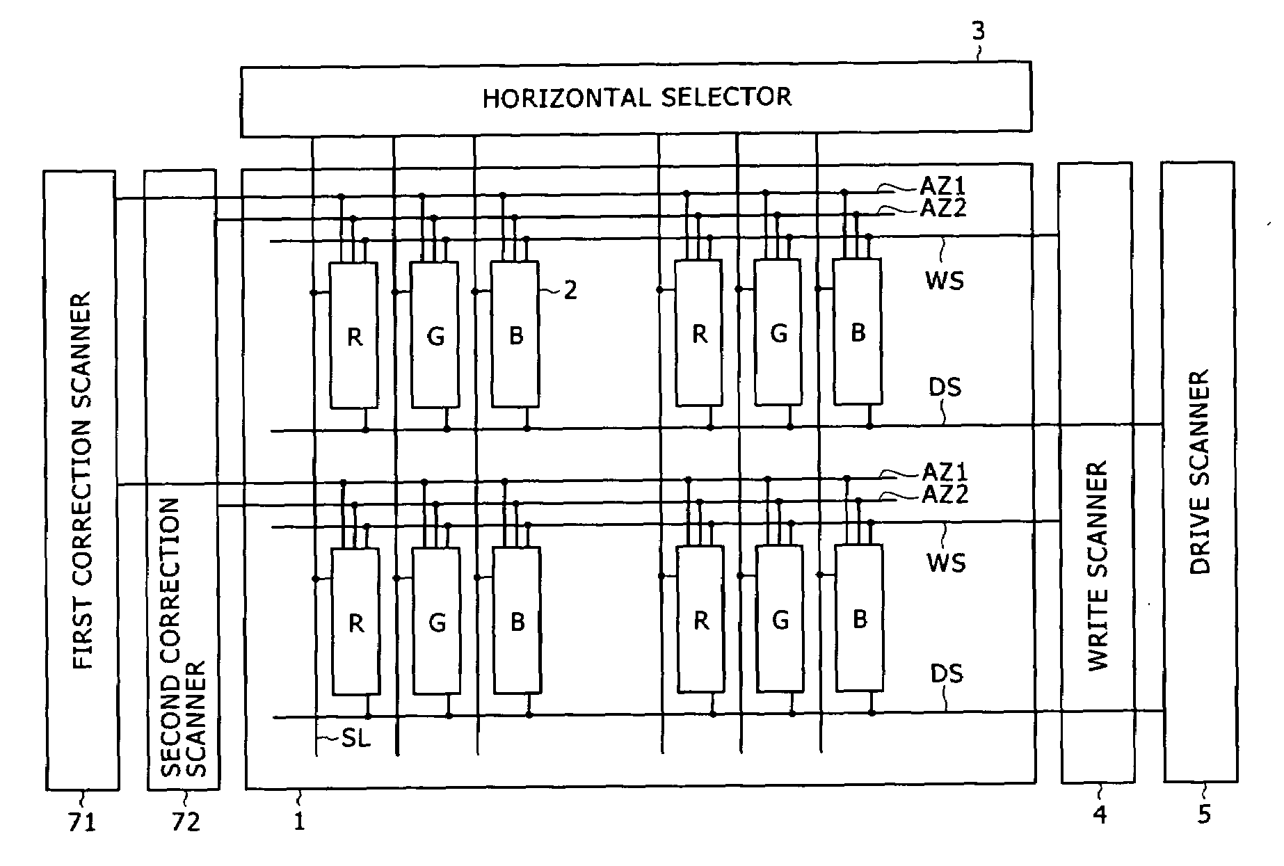
[0016]There is a need for the present invention to provide a display device that can accelerate mobility correction operation so that mobility correction can be carried out in a short time. There is another need for the present invention to provide a display device that can adjust a mobility correction period depending on the
grayscale (
signal level) of a video signal. According to a first mode of the present invention, there is provided a display device including a
pixel array part configured to include scan lines disposed along rows,
signal lines disposed along columns, and pixels that are disposed at the intersections of the scan lines and the
signal lines and are arranged in a matrix, and a drive part configured to have at least a write
scanner that sequentially supplies a
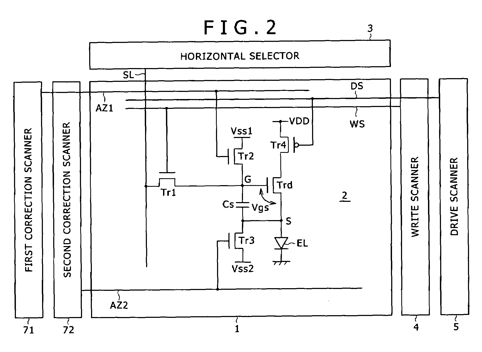
control signal to the scan lines to thereby carry out line-sequential scanning and a signal selector that supplies a video signal to the signal lines in matching with the line-sequential scanning. Each of the pixels includes at least a sampling transistor, a drive transistor, a holding capacitor, and a light-emitting element. A control terminal of the sampling transistor is connected to the
scan line, and a pair of current terminals of the sampling transistor are connected between the signal line and a control terminal of the drive transistor. One of a pair of current terminals of the drive transistor is connected to the light-emitting element, and the other of the pair of current terminals of the drive transistor is connected to a power supply. The holding capacitor is connected between the control terminal of the drive transistor and the current terminal of the drive transistor. The sampling transistor is turned on in response to a
control signal supplied to the
scan line to thereby sample a video signal from the signal line and write the video signal to the holding capacitor, and the sampling transistor carries out negative feedback of a current that flows from the drive transistor to the holding capacitor to thereby write a correction amount dependent upon the mobility of the drive transistor to the holding capacitor in a predetermined correction period until the sampling transistor is turned off in response to a control signal. The drive transistor supplies, to the light-emitting element, a current dependent upon the video signal and the correction amount written to the holding capacitor to thereby cause the light-emitting element to emit light. The write
scanner supplies a control signal including at least double pulses to the
scan line to thereby set a first correction period, a second correction period, and a correction intermediate period between the first correction period and the second correction period. The sampling transistor carries out writing of a correction amount to the holding capacitor in the first correction period and accelerates the writing of the correction amount to the holding capacitor in the correction intermediate period, and the sampling transistor settles the writing of the correction amount to the holding capacitor in the second correction period.
[0017]According to a second mode of the present invention, there is provided a display device including a
pixel array part configured to include scan lines disposed along rows, signal lines disposed along columns, and pixels that are disposed at the intersections of the scan lines and the signal lines and are arranged in a matrix, and a drive part configured to have at least a write scanner that sequentially supplies a control signal to the scan lines to thereby carry out line-sequential scanning and a signal selector that supplies a video signal to the signal lines in matching with the line-sequential scanning. Each of the pixels includes at least a sampling transistor, a drive transistor, a holding capacitor, and a light-emitting element. A control terminal of the sampling transistor is connected to the scan line, and a pair of current terminals of the sampling transistor are connected between the signal line and a control terminal of the drive transistor. One of a pair of current terminals of the drive transistor is connected to the light-emitting element, and the other of the pair of current terminals of the drive transistor is connected to a power supply. The holding capacitor is connected between the control terminal of the drive transistor and the current terminal of the drive transistor. The sampling transistor is turned on in response to a control signal supplied to the scan line to thereby sample a video signal from the signal line and write the video signal to the holding capacitor, and the sampling transistor carries out negative feedback of a current that flows from the drive transistor to the holding capacitor to thereby write a correction amount dependent upon the mobility of the drive transistor to the holding capacitor in a predetermined correction period until the sampling transistor is turned off in response to a control signal. The drive transistor supplies, to the light-emitting element, a current dependent upon the video signal and the correction amount written to the holding capacitor to thereby cause the light-emitting element to emit light. The write scanner supplies, to the scan line, a control signal including at least double pulses having peak levels different from each other. The sampling transistor is turned on and off in accordance with the peak levels of the double pulses applied to the control terminal of the sampling transistor as the gate of the sampling transistor depending on the level of a video signal applied to the current terminal of the sampling transistor as the source of the sampling transistor, to thereby automatically adjust a correction time depending on the level of the video signal.
[0018]According to the first mode of the present invention, the write scanner supplies a control signal including double pulses to the scan line to thereby set the first correction period, the second correction period, and the correction intermediate period between these correction periods. The sampling transistor carries out writing of a correction amount to the holding capacitor in the first correction period, and accelerates the writing of the correction amount to the holding capacitor in the correction intermediate period. Furthermore, the sampling transistor settles the writing of the correction amount to the holding capacitor in the second correction period. In this manner, the correction period is divided into at least the former period and the latter period, and the writing of the correction amount is accelerated in the correction intermediate period between the former and latter periods. This feature allows shortening of the entire correction time, which can provide compatibility with enhancement in the definition and the
pixel density of the display device.
[0019]According to the second mode of the present invention, the write scanner supplies, to the scan line, a control signal including at least double pulses having peak levels different from each other. The sampling transistor is turned on and off in accordance with the peak levels of the double pulses applied to the gate thereof depending on the level of the video signal applied to the source thereof, to thereby automatically adjust the mobility correction time depending on the level of the video signal. This feature makes it possible to automatically adjust the mobility correction time to the optimum time depending on the level of the video signal, and thus can achieve image displaying with high uniformity for all of the grayscales of the video signal.

