Electronic Device, Multilayer Ceramic Capacitor and the Production Method Thereof

a multi-layer ceramic capacitor and production method technology, applied in the direction of fixed capacitors, stacked capacitors, fixed capacitor details, etc., can solve the problems of reducing the capacitance of multi-layer ceramic capacitors, and affecting the sintering temperature of both. , to achieve the effect of suppressing the growth of conductive particles, preventing the spheroidization of fired internal electrode layers and the breaking of electrodes

Inactive Publication Date: 2009-05-14
TDK CORPARATION
View PDF4 Cites 14 Cited by
  • Summary
  • Abstract
  • Description
  • Claims
  • Application Information

AI Technical Summary

Benefits of technology

[0060]According to the present invention, it is possible to suppress grain growth of conductive particles in the firing step, effectivel...

Problems solved by technology

However, since nickel has a lower melting point comparing with that of the dielectric powder included in the pre-fired dielectric layers, when firing the pre-fired dielectric layers and pre-fired internal electrode layers at a time, there arises a difference in sintering temperatures of the both.
In the case where the sintering temperatures are largely different as such, when firing is performed at a high temperature, nickel particles included in the conductive material become spheroidized due to grain growth and cavities arise at arbitrary places, consequently, it becomes difficul...

Method used


Image

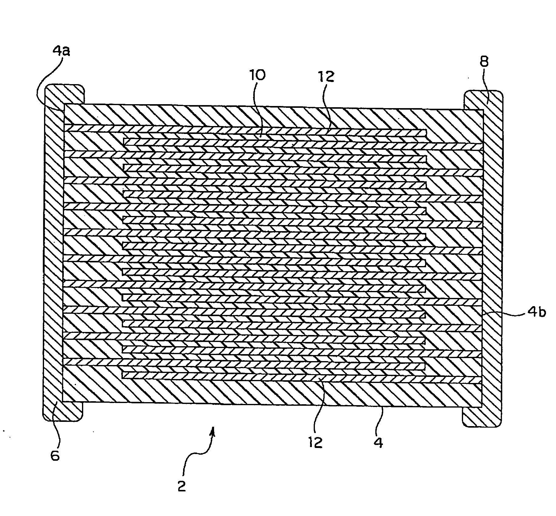
  • Electronic Device, Multilayer Ceramic Capacitor and the Production Method Thereof
  • Electronic Device, Multilayer Ceramic Capacitor and the Production Method Thereof
  • Electronic Device, Multilayer Ceramic Capacitor and the Production Method Thereof

Examples


example 1

Production of Respective Paste

[0142]First, a BaTiO3 powder (BT-02 made by Sakai Chemical Industry Co., Ltd.), MgCO3, MnCO3, (Ba0.6Ca0.4)SiO3 and a powder selected from rare earths (Gd2O3, Tb4O7, Dy2O3, Ho2O3, Er2O3, Tm2O3, Yb2O3, Lu2O3 and Y2O3) were wet mixed by a ball mill for 16 hours and dried to obtain a dielectric material. An average particle diameter of these material powders was 0.1 to 1 μm. The (Ba0.6Ca0.4)SiO3 was produced by wet mixing BaCo3, CaCO3 and SiO2 by a ball mill for 16 hours, drying, then, firing at 1150° C. in the air, and dry pulverizing the result by a ball mill for 100 hours.

[0143]To make the obtained dielectric material to be paste, an organic vehicle was added to the dielectric material and mixed by a ball mill, so that dielectric green sheet paste was obtained. The organic vehicle has a compounding ratio of polyvinyl butyral as a binder in an amount of 6 parts by weight, bis(2-ethylhexyl)phthalate (DOP) as a plasticizer in an amount of 3 parts by weight,...

example 2

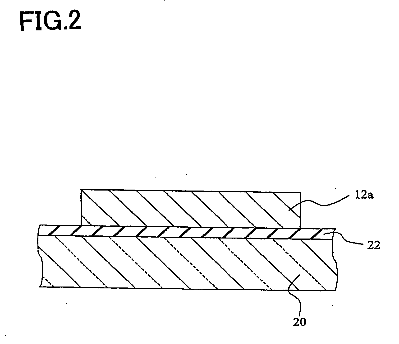
[0191]The dielectric green sheet paste produced in the example 1 was applied to the PET film (carrier sheet) by using a wire bar coater and, then, dried to obtain a green sheet 10a. A pre-fired internal electrode thin film 12a was formed on the green sheet 10a in the same way as in the example 1 and a multilayer body as shown in FIG. 8 was produced. Next, the PET film was removed from the multilayer body to produce a pre-fired sample composed of the green sheet 10a and the internal electrode thin film 12a. The pre-fired sample was subjected to binder removal, firing and annealing in the same way as in the example 1, so that a sample for surface observation after firing composed of the dielectric layers 10 and the internal electrode layers 12 was produced.

[0192]Next, SEM observation was made on the obtained surface observation sample from the vertical direction with respect to the surface formed with the internal electrode layer 12, and the fired internal electrode layer was observed...

example 3

[0195]Other than using Yb2O3 instead of BaTiO3 as a dielectric target when forming the pre-fired internal electrode thin film 12a, samples were obtained in the same way as in the example 1. An evaluation of electric characteristics (capacitance C and dielectric loss tan δ) was made on each sample. The results are shown in Table 2. The electric characteristics (capacitance C and dielectric loss tan δ) were evaluated in the same way as in the example 1.

TABLE 2Pre-Fired Internal Electrode Thin Film 12aContent RatioContent RatioSampleThicknessof Nickelof BaTiO3CapacitanceNo.[μm][mol %][mol %][μF]tan δEvaluation6Comparative0.4100.000.00.830.01XExample7Example0.499.300.700.970.02◯8Example0.498.101.900.950.02◯9Example0.497.003.000.920.02◯10Comparative0.494.865.140.740.02XExample

[0196]Table 2 shows a thickness of a pre-fired internal electrode thin film 12a formed for each sample, a content ratio of nickel and Yb2O3, capacitance, dielectric loss tan δ and evaluation on each sample.

[0197]As ...


PUM

PropertyMeasurementUnit
Temperatureaaaaaaaaaa

Abstract

An electronic device, such as a multilayer ceramic capacitor, and a method for producing the electronic device having an internal electrode layer and a dielectric layer, comprising a step of forming a pre-fired internal electrode thin film including a conductive component and a dielectric component, a step of stacking green sheets to be dielectric layers after firing and the internal electrode thin films, and a step of firing a multilayer body of the green sheets and the internal electrode thin films are provided: by which grain growth of conductive particles in a firing step can be suppressed, spheroidizing in the internal electrode layers and breaking of electrodes can be effectively prevented, and a decline of the capacitance can be effectively suppressed even when a thickness of each internal electrode layer is made thinner.

Description

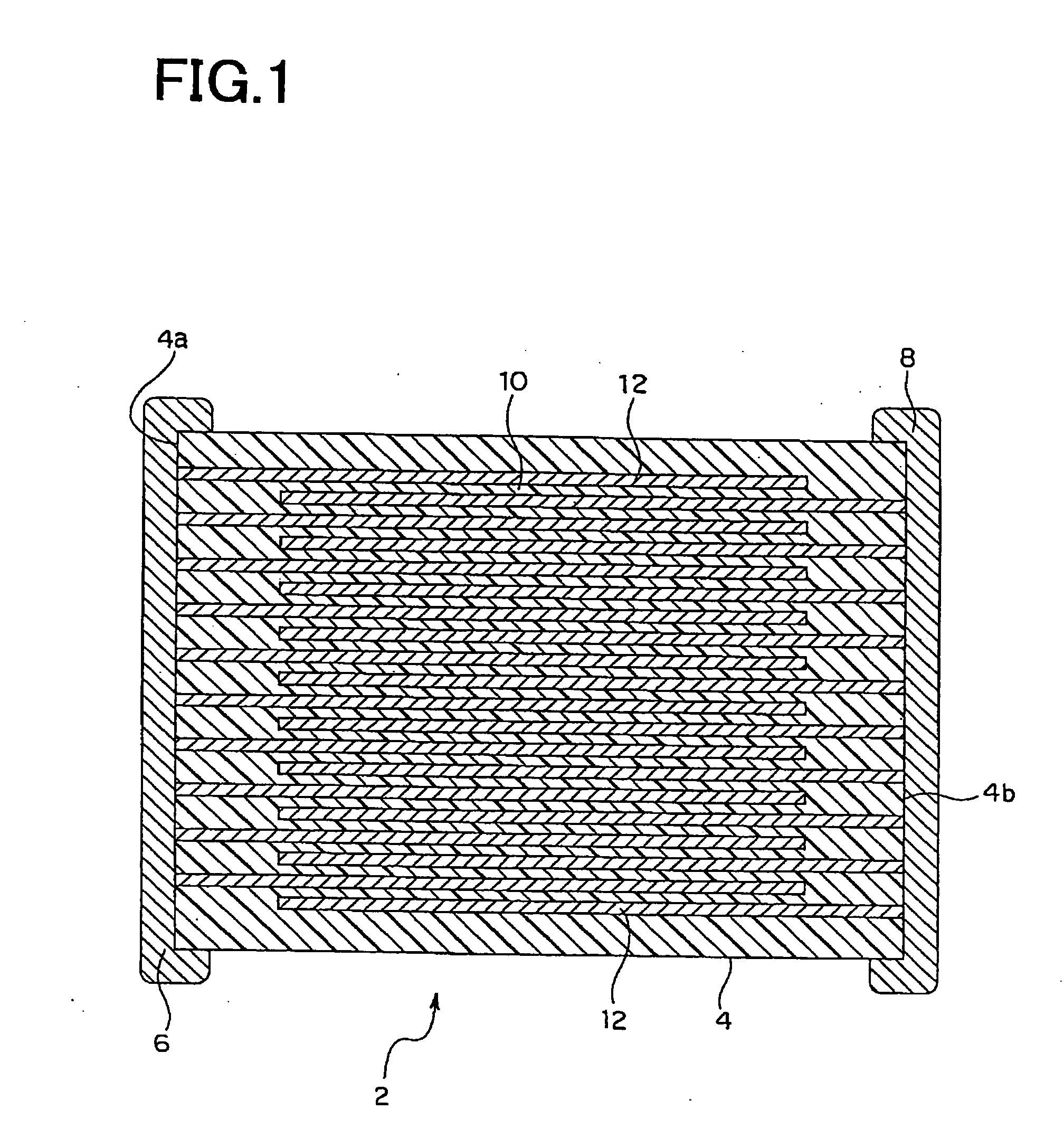
BACKGROUND OF THE INVENTION[0001]1. Field of the Invention[0002]The present invention relates to an electronic device, a multilayer ceramic capacitor and the production method and, particularly, relates to an electronic device and a multilayer ceramic capacitor capable of responding to attaining a thinner layers and downsizing.[0003]2. Description of the Related Art[0004]A multilayer ceramic capacitor as an example of electronic devices comprises an element body having a multilayer structure, wherein a plurality of dielectric layers and internal electrode layers are alternately arranged, and a pair of external terminal electrodes formed on both ends of the element body.[0005]The multilayer ceramic capacitor is produced by forming a pre-fired element body by alternately stacking a plurality of pre-fired dielectric layers and pre-fired internal electrode layers exactly by necessary numbers, firing the result and, then, forming a pair of external terminal electrodes on both end portion...

Claims


Application Information

Patent Timeline
IPC IPC(8): H01G4/12B32B37/06H01G4/008H01G4/30
CPCH01G4/0085H01G4/30H01G4/1227H01G4/1209H01G4/12
Inventor SUZUKI, KAZUTAKASATO, SHIGEKI
Owner TDK CORPARATION
Why Eureka
Try Eureka