Semiconductor device having trench extending perpendicularly to cleaved plane and manufacturing method of the same

a technology of semiconductor devices and cleaved planes, which is applied in the direction of semiconductor devices, lasers, semiconductor lasers, etc., can solve the problems of easy cracks along the cleaved plane, and increasing the number of steps, so as to reduce the yield

Inactive Publication Date: 2009-05-14
ROHM CO LTD
View PDF0 Cites 11 Cited by
  • Summary
  • Abstract
  • Description
  • Claims
  • Application Information

AI Technical Summary

Problems solved by technology

Thus, when the substrate surface is marked off along a plane other than the substrate of the hexagonal structure and the cleaved plane of the semiconductor film crystal-grown on the substrate, cracks easily occur along the cleaved plane.
Especially, in a semiconductor device of a ridge structure, it is often the case that cracks occur in a surface of the semiconductor device from a marked-off portion to a step portion of the ridge.
However, the aforementioned method increases the number of steps by adding the step of forming the split slots.
Besides, when the split slots are formed, cracks occur or the wafer is split to cause a reduction in yield of the semiconductor device.

Method used


Image

  • Semiconductor device having trench extending perpendicularly to cleaved plane and manufacturing method of the same
  • Semiconductor device having trench extending perpendicularly to cleaved plane and manufacturing method of the same
  • Semiconductor device having trench extending perpendicularly to cleaved plane and manufacturing method of the same

Examples


first embodiment

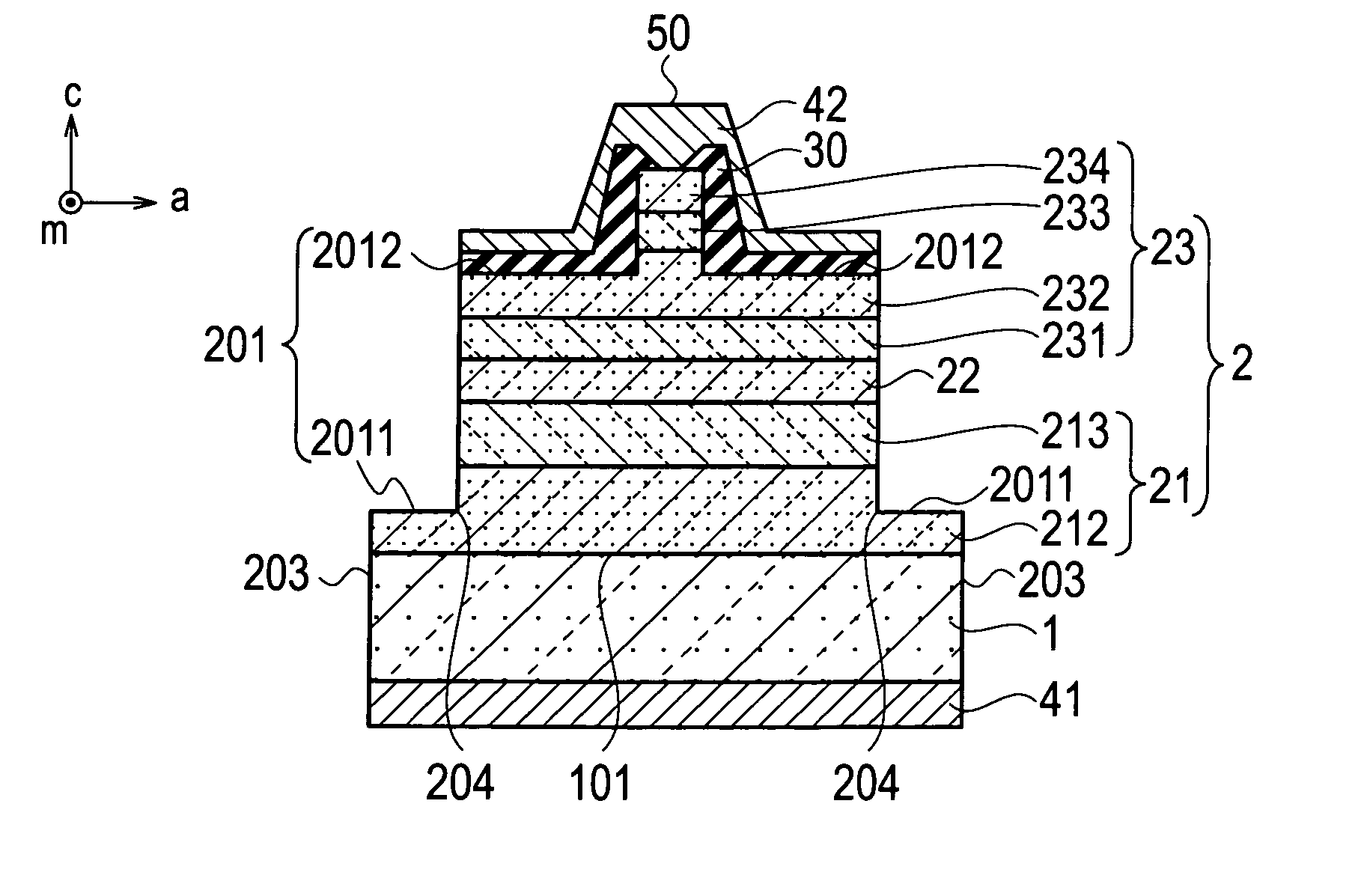
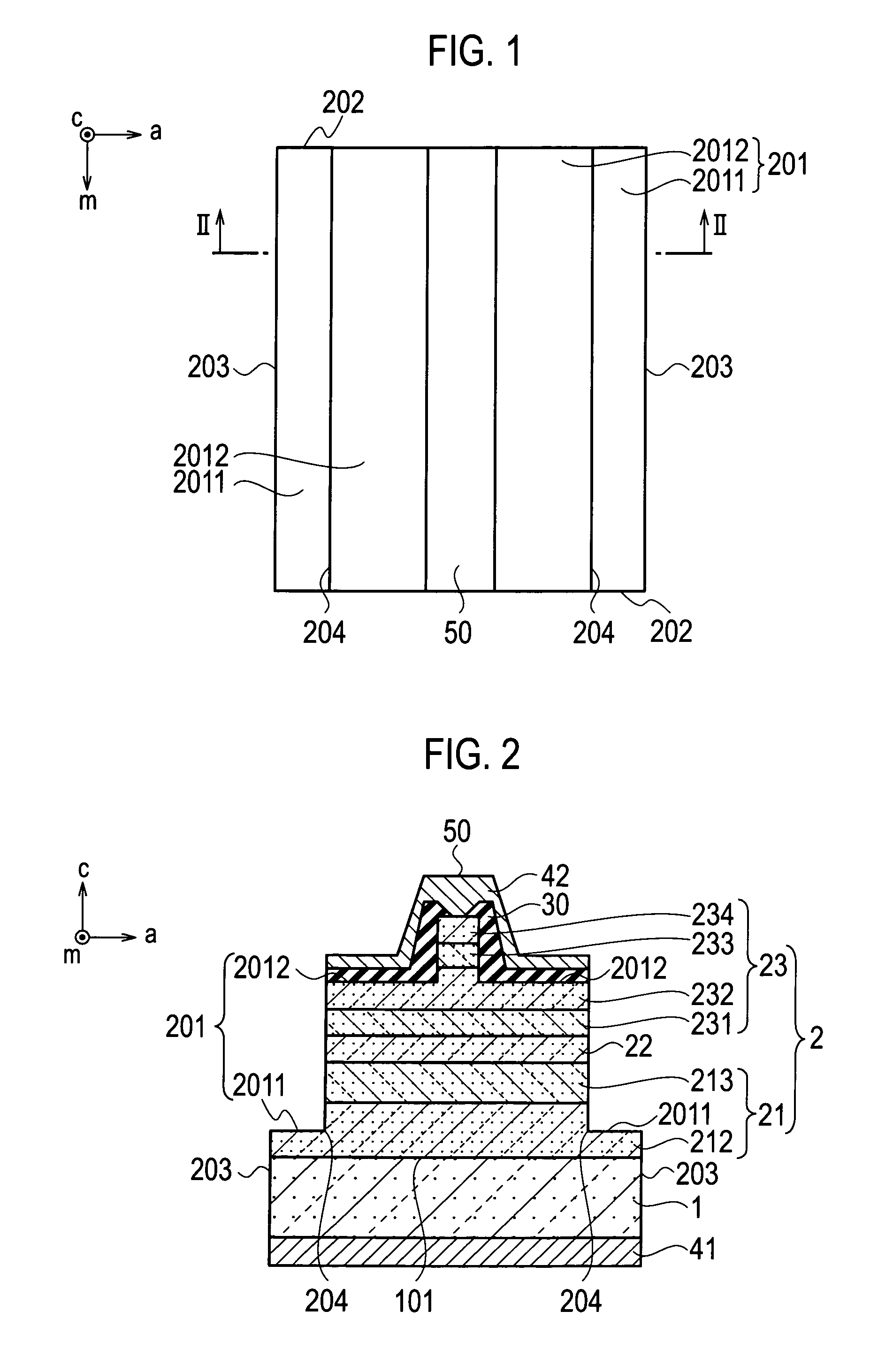
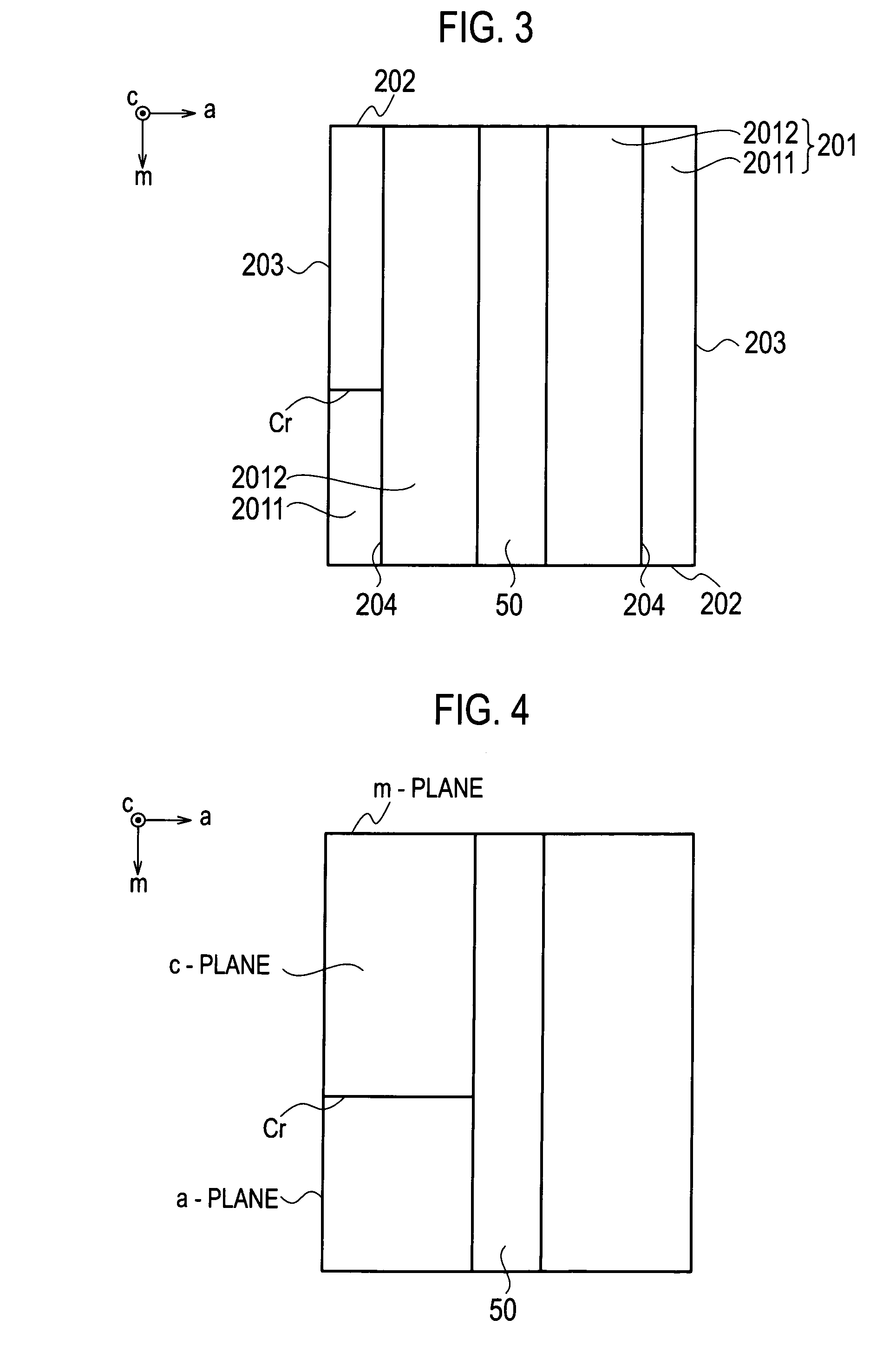
[0027]According to a first embodiment of the present invention, as illustrated in a top view of FIG. 1 and a sectional view of FIG. 2 cut along the line II-II of FIG. 1, a semiconductor device includes a substrate 1 constituted of a semiconductor of a hexagonal structure and having a substrate principal plane 101 which is a polar plane, and a semiconductor layer 2 constituted of a nitride-base compound semiconductor of a hexagonal structure disposed on the substrate principal plane 101 and having a principal plane 201 which is a polar plane, an m-side face 202 which is a (1-100) plane (m-plane) orthogonal to the principal plane, and an a-side face 203 which is a (11-20) plane (a-plane) orthogonal to the (1-100) plane, the faces 202 and 203 being arranged adjacently to the principal plane, and where an outer edge portion of a section along the (1-100) plane is mesa-shaped. FIG. 2 is a sectional view cut along the (1-100) plane of the semiconductor device illustrated in FIG. 1. The he...

second embodiment

[0066]As illustrated in a top view of FIG. 8, and a sectional view of FIG. 9 cut along the line IX-IX of FIG. 8, a semiconductor device of a second embodiment of the present invention is different from the semiconductor device illustrated in FIGS. 1 and 2 in that an outer edge portion of a section along an a-side face 203 as an a-plane orthogonal to a principal plane 201 of a semiconductor layer 2 is mesa-shaped except for an area where a ridge stripe 50 is formed. In other words, in the outer edge portion of the principal plane 201 of the semiconductor layer 2, an area except for the area of the ridge stripe 50 is mesa-etched to form a step portion 204. Other components are similar to those of the first embodiment illustrated in FIGS. 1 and 2.

[0067]In the case of the semiconductor device illustrated in FIGS. 1 and 2, in the outer edge portion of the principal plane 201 of the semiconductor layer 2, the area along the a-side face which is an a plane is mesa-etched to form the step p...


PUM


Abstract

A method for manufacturing a semiconductor device includes setting cut lines in parallel to a normal direction of a (1-100) plane orthogonal to the principal plane and in parallel to a normal direction of a (11-20) plane orthogonal to the (1-100) plane; forming, along the cut line parallel to the normal direction of the (1-100) plane, a trench from the principal plane of the semiconductor layer to a midpoint of a boundary plane between the semiconductor layer and the substrate; and cutting the wafer along the cut lines to divide the wafer into the plurality of semiconductor device where four side faces which are nonpolar planes orthogonal to the principal plane are set adjacent to the principal plane.

Description

CROSS REFERENCE TO RELATED APPLICATIONS AND INCORPORATION BY REFERENCE[0001]This application is based upon and claims the benefit of priority from prior Japanese Patent Application P2007-239642 filed on Sep. 14, 2007; the entire contents of which are incorporated by reference herein.BACKGROUND OF THE INVENTION[0002]1. Field of the Invention[0003]The present invention relates to a semiconductor device including a substrate of a hexagonal structure, and manufacturing method of the same.[0004]2. Description of the Related Art[0005]Generally, to divide a substrate having a semiconductor film formed therein to manufacture a chip, division by dicing or cleaving by a scriber is used. In the case of division by dicing, for example, the substrate is cut from its back or front by a blade rotated fast at one or multiple stages to be divided. In the case of cleaving by a scriber, a trench is formed in the substrate by a pen or the like having a diamond disposed in its tip, and the substrate is ...

Claims


Application Information

Patent Timeline
Patent Type & Authority Applications(United States)
IPC IPC(8): H01S5/323H01L21/304H01L29/15H01L33/16H01L33/32
CPCH01L33/0095H01S5/32341H01S5/22
Inventor MURAYAMA, MASAHIRO
Owner ROHM CO LTD
Why Eureka
Try Eureka