Antenna Configurations for Compact Device Wireless Communication

a wireless communication and compact device technology, applied in diversity/multi-antenna systems, duplex signal operation, polarisation/directional diversity, etc., can solve the problems of reducing the overall received radio throughput, signal strength degradation, and reducing so as to reduce the overall antenna dipole arm length, reduce current density, and reduce the effect of sar

Inactive Publication Date: 2009-05-14
SIERRA WIRELESS
View PDF54 Cites 190 Cited by
  • Summary
  • Abstract
  • Description
  • Claims
  • Application Information

AI Technical Summary

Problems solved by technology

Some computing devices, such as laptop computers, may not be manufactured with wireless communication capability.
The antennas can be spatially separated and / or use orthogonal polarizations (i.e. vertical and horizontal polarizations, right and left circular polarization, etc.) During a fade, the signal strength is degraded to the point that long error bursts occur in the received signal, severely degrading the overall received radio throughput, amongst other degradations.
One of the main disadvantages of these sample diversity systems is the generally poor isolation between the antennas, sometimes as low as a few dB but typically only 6 dB.
Small form factor wireless communications devices, such as PCMCIA cards, provide very limited external space to include antennas with high efficiency, wide bandwidth, multiple bands and diversity all at the same time.
This tight space constraint results in interaction between the various antenna elements, even if the antennas have good isolation between the selected paths or “ports.” This is further complicated by the interaction between the various antenna systems and the computer or platform to which the card is mated.
Since the FCC part 15 requires only radiated noise limitations, the issue of self-noise for added or integrated wireless network solutions has not been considered.
Radiation in the PCMCIA slot regions may be substantially vertically polarized, and conduction currents from the laptop chassis generate conduction noise into antenna structures, such as the traditional monopole, that use the chassis as the substantial counterpoise for the antenna.
With the exception of the end-fed dipole antenna, all of the antennas of FIG. 12a-12c suffer from conducted RF noise from the chassis or ground plane of the computer.
The extent of the projection of a PCMCIA card outside the slot in the side of the laptop is primarily limited by aggressively small industrial design (ID) constraints that have little concern for the needs of RF antenna functionality.
Additional constraints are imposed by the mechanical enclosure and its requirements for welding line wall thickness and studs and so forth.
In addition, the location of a dipole antenna near a significant ground plane also impacts the bandwidth and performance of a dipole antenna.
The very nature of this three-element Yagi design renders a 0.824 GHz solution extremely inefficient and / or limited bandwidth.
This is a particularly important mobile phone issue as the transceivers of the device are employed in close proximity to the operator's head.
While these seem like simple remedies they each come with a cost, and a trade-off is required that usually impacts either industrial design (ID) and / or antenna and system performance.
This latter application, if used at all, has mostly been used at 1.8 GHz and above, due the unacceptable size of the antenna at lower frequencies such as 850 MHz.
However, such air-cored transformers have significantly more flux leakage than a high Mu ferrite-cored transformer.
The main issue is that if the leakage (uncoupled) inductance exceeds the mutual inductance, the capacitive tuning required will result in a narrower band coupling.
The perceived disadvantage is the leakage inductance and the size of the coupling loops, which is directly related to the maximum operating wavelength.

Method used


Image

  • Antenna Configurations for Compact Device Wireless Communication
  • Antenna Configurations for Compact Device Wireless Communication
  • Antenna Configurations for Compact Device Wireless Communication

Examples


Embodiment Construction

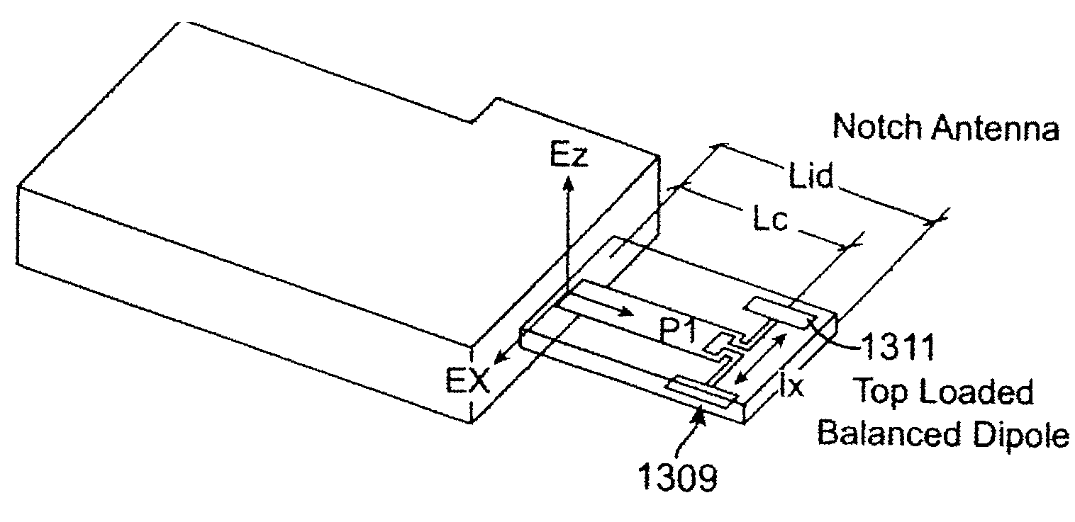
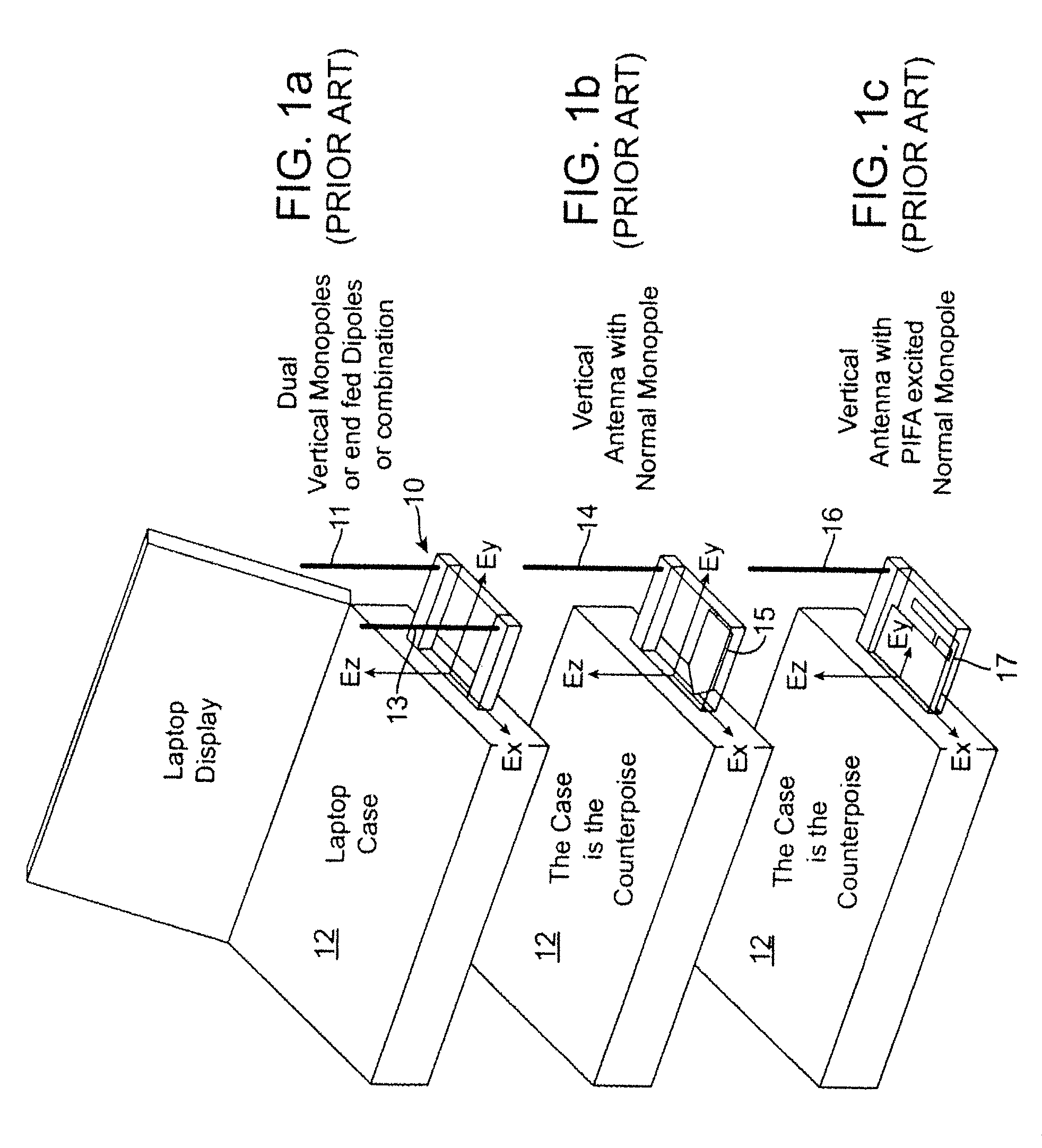
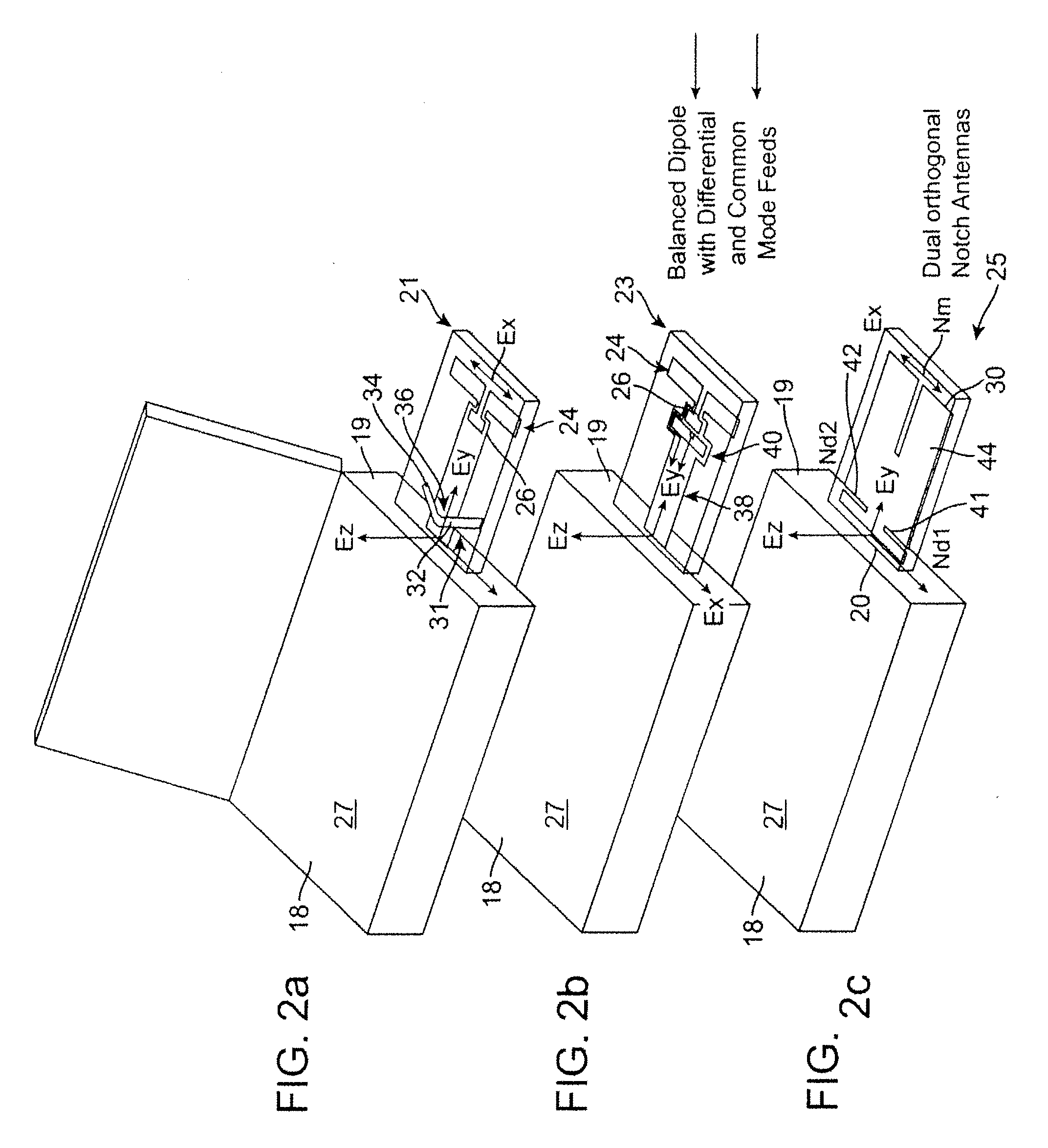
[0067]The description herein is provided in the context of antenna configurations for compact device wireless communication. While explained in terms of a laptop computer as a host device, and a PCMCIA or similar PC card as the wireless communication device, it will be appreciated that the invention is not so limited, and other host devices, such as PDAs and desktop computers, and other wireless communication devices for establishing wireless communication through a cellular network or through Bluetooth™, WiFi™ and other types of wireless links and channels are also contemplated. Moreover, the principles of the invention are not restricted to communication devices that are designed to mate with host devices to provide wireless capability thereto, but are more generally applicable to cellular telephones, two-way radios, and other self-contained wireless communication devices that may be equipped with their own antennas or antenna systems.

[0068]Those of ordinary skill in the art will ...


PUM


Abstract

A wireless communication device is configured to provide wireless communication to a host device when disposed in a mated position with the host device. The wireless communication device includes a transceiver, a controller in communication with the transceiver, and a modem in communication with the controller. The wireless communication device further includes a printed circuit board (PCB) having a first inductor loop, and an antenna having second inductor loop inductively coupled with the first inductor loop.

Description

CROSS REFERENCE TO RELATED APPLICATIONS[0001]This application claims the benefit of U.S. Provisional Patent Application No. 60 / 967,449, filed on Sep. 4, 2007, entitled “Antenna Systems”, the disclosure of which is hereby incorporated by reference for all purposes.BACKGROUND OF THE INVENTION[0002]1. Field of the Invention[0003]The invention relates to antennas for use with portable and other computing devices, such as laptop computers. More specifically, it relates to antennas that may be part of removable components such as PCMCIA (personal computer memory card international association) cards or the like that provide wireless communication to the computing devices.[0004]2. Description of the Related Art[0005]Some computing devices, such as laptop computers, may not be manufactured with wireless communication capability. Rather, some of these devices may have slots or similar coupling locations into which wireless communication devices may be mated to provide the host computing devi...

Claims


Application Information

Patent Timeline
Patent Type & Authority Applications(United States)
IPC IPC(8): H04B1/38
CPCH01Q1/38H04B7/10H01Q9/285H01Q1/2275
Inventor NYSEN, PAUL A.
Owner SIERRA WIRELESS
Why Eureka
Try Eureka