Method for forming interlayer dielectric film, interlayer dielectric film, semiconductor device and semiconductor manufacturing apparatus

Active Publication Date: 2009-05-21
RENESAS ELECTRONICS CORP
View PDF55 Cites 1 Cited by
  • Summary
  • Abstract
  • Description
  • Claims
  • Application Information

AI Technical Summary

Problems solved by technology

Some interlayer dielectric films obtained using these methods are reported to have dielectric constants of 2.4 or less; however, due to reduced mechanical strength caused by an increase in pores or hydrocarbons, the interlayer dielectric films have the problem of lowered reliability due to removal during the semiconductor process.
An increase in pores or hydrocarbons causes not only lowered mechanical strength but also the adsorption of moisture in the atmosphere.
In addition, the adsorbed moisture causes the decomposition of hydrocarbons, which is one cause of an increased dielectric constant.
In particular, when a film is formed by the plasma CVD method, decomposition products of raw materials due to plasma reactions are not terminated, possibly resulting in sites where moisture is adsorbed.
Using the technique described in Japanese Patent Laid-Open No. 11-330070, however, the formation of a film using a hydrogen reaction is difficult to control because the system is complicated due to the introduction of two types of gases, and the reduction of the film itself is induced.
Moreover, even if purging with an inert gas is performed prior to film formation, as described in Japanese Patent Laid-Open No. 2006-253290, it is impossible to remove the reaction products formed during the subsequent formation of an interlayer dielectric film, consequently causing the dielectric constant of the film to change over time.

Method used


Image

  • Method for forming interlayer dielectric film, interlayer dielectric film, semiconductor device and semiconductor manufacturing apparatus
  • Method for forming interlayer dielectric film, interlayer dielectric film, semiconductor device and semiconductor manufacturing apparatus
  • Method for forming interlayer dielectric film, interlayer dielectric film, semiconductor device and semiconductor manufacturing apparatus

Examples


first exemplary embodiment

[0019]The best mode for carrying out the invention is next described using the drawings.

[0020]A monomer with an unsaturated hydrocarbon is used as a raw material to form an interlayer dielectric film. Examples of monomers with an unsaturated hydrocarbon include monomers with a 3-membered ring of SiO (Formula 1), monomers with a 4-membered ring of SiO (Formula 5), and monomers with a straight-chain structure (Formula 10):

[0021]In the monomers with an unsaturated hydrocarbon with the above-described 3-membered ring represented by Formula 1, R1 is an unsaturated carbon compound; R2 is a saturated carbon compound; R1 is a vinyl group or an allyl group; and R2 is any of a methyl, an ethyl group, a propyl group, an isopropyl group, and a butyl group.

[0022]In the monomers with an unsaturated hydrocarbon with the above-described 4-membered ring represented by Formula 5, R3 is an unsaturated carbon compound; R4 is a saturated carbon compound; R1 is a vinyl group or an allyl group; and R2 is ...

example 1

[0029]Example 1 using the first exemplary embodiment is next described using the drawings. Examples of raw-material monomers that can be used to form an interlayer dielectric film include the following shown below. Monomers with a 3-membered ring of SiO represented by (Formula 2) to (Formula 4) can be used as monomers:

[0030]Monomers with a 4-membered ring of SiO represented by (Formula 6) to (Formula 9) can be used as raw materials:

[0031]Straight-chain monomers with a structure represented by (Formula 11) can be used as raw materials:

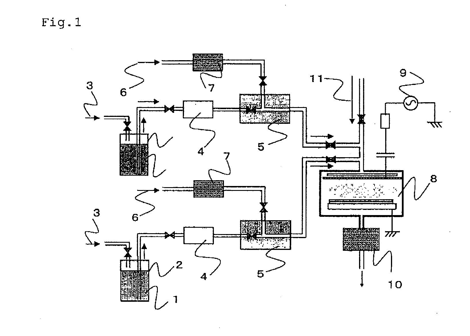
[0032]The above-described raw-material monomer 1 charged in the monomer reservoir 2 is discharged therefrom via the pressure-fed gas 3, and the liquid mass flow 4 controls the flow rate of the raw-material monomer 1. The flow rate-controlled raw-material monomer 1 receives heat from a heater (not shown) in the vaporizer 5 and is thereby vaporized. The vaporized gas is mixed in the vaporizer 5 with the carrier gas 6 whose flow rate is controlled by the m...

second exemplary embodiment

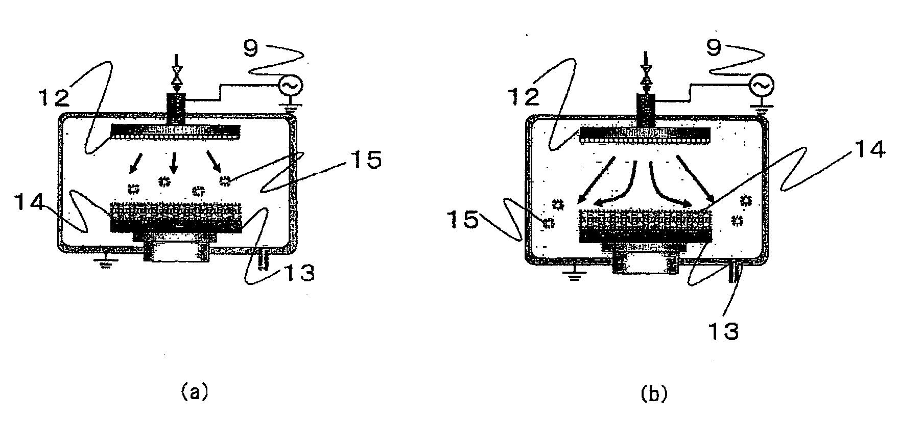
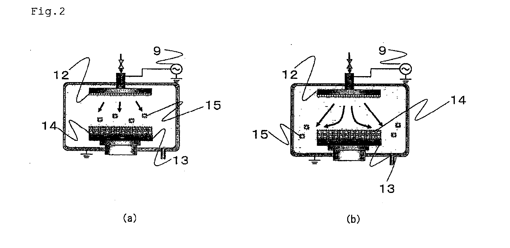
[0037]A second exemplary embodiment for carrying out the invention is next described using the drawings.

[0038]Subsequent to forming an interlayer dielectric film on a substrate 14 as in the first embodiment, an inert gas was introduced to plasma-treat the surface of the interlayer dielectric film. This process is illustrated in FIG. 7. After forming the film, the introduction of the raw-material monomer and that of the carrier gas were stopped simultaneously, and then an inert gas was introduced. After stabilization, a plasma was generated to perform a treatment. He was used as the inert gas, and the treatment was performed in the reactor at a pressure of 800 Pa and an RF power of 400 W for 10 to 60 seconds. The treatment conditions vary depending on the size of the reactor, the type of the inert gas, and the type of the raw-material monomer, and cannot therefore be determined unequivocally. After the plasma treatment using the inert gas, purging was performed under conditions such ...


PUM

PropertyMeasurementUnit
Temperatureaaaaaaaaaa
Timeaaaaaaaaaa
Dielectric polarization enthalpyaaaaaaaaaa

Abstract

A method for forming an interlayer dielectric film by a plasma CVD method, including turning off a radio frequency power and purging with an inert gas simultaneously.

Description

[0001]This application is; based upon and claims the benefit of priority from Japanese patent application No. 2007-240721, filed on Sep. 18, 2007, the disclosure of which is incorporated herein in its entirety by reference.BACKGROUND OF THE INVENTION[0002]1. Field of the Invention[0003]The present invention relates to a method for forming an interlayer dielectric film, an interlayer dielectric film, a semiconductor device, and a semiconductor manufacturing apparatus; and particularly to a method for forming an interlayer dielectric film in which change over time is reduced, and an interlayer dielectric film formed by the method.[0004]2. Description of the Related Art[0005]Conventionally, silica (SiO2) has been widely used as an interlayer dielectric material for use in the copper wiring layer of semiconductor devices. As semiconductor devices have become miniaturized and increased in speed, however, films with lower dielectric constants have increasingly been used as interlayer diel...

Claims


Application Information

Patent Timeline
IPC IPC(8): H01L29/06C23C16/44B32B27/06H01L21/31
CPCC23C16/401H01L21/02126H01L21/02216H01L23/5329H01L21/0234H01L21/3122H01L21/76801H01L21/02274H01L2924/0002Y10T428/31667H01L2924/00
Inventor YAMAMOTOITO, FUMINORIHAYASHI, YOSHIHIRO
Owner RENESAS ELECTRONICS CORP
Why Eureka
Try Eureka