Power Device Packages and Methods of Fabricating the Same

a technology of power device and package, which is applied in the direction of semiconductor devices, semiconductor/solid-state device details, electrical apparatus, etc., can solve the problems of shortening the life of the power device package, easy deterioration of electrical and mechanical reliability, and inability to obtain the desired compact power device package, etc., and achieves excellent compatibility and simplified wiring process for electric connection between stacked power semiconductor chips.

Active Publication Date: 2009-05-21
SEMICON COMPONENTS IND LLC
View PDF8 Cites 17 Cited by
  • Summary
  • Abstract
  • Description
  • Claims
  • Application Information

AI Technical Summary

Benefits of technology

[0008]Aspects of the present invention provide power device packages in which a wiring process for electric connection between stacked power semiconductor chips can be simplified, wherein the stacked power device packages have excellent compatibility with power semiconductor chips whose lower surface is used as electrodes, and the electric and mechanical characteristics of the power device packages cannot be easily deteriorated due to heat during the operation thereof.
[0009]Aspects of the present invention also provide methods of manufacturing the power device packages having the above-described advantages at low cost.

Problems solved by technology

However, since the footprint area of the conventional power device package is increased as the number of mounted semiconductor chips increases, a desired compact power device package cannot be obtained.
In addition, as the volume of the conventional power device package is increased, its electrical and mechanical reliability may be readily deteriorated due to temperature cycles that are repeated in a range of high temperature, and the life span of the power device package may be shorted.
However, the cost for manufacturing the stacked power device package is relatively high because the wiring process for electrical connection between the stacked power semiconductor chips is complicated and expensive.
Also, since vertical type power semiconductor devices such as insulated-gate bipolar transistors (IGBTs), metal-oxide-semiconductor (MOS) transistors, power diodes, power regulators, etc. use a lower surface of semiconductor chips as a drain electrode or a ground electrode, it is difficult to stack the power device chips into a power device package.

Method used


Image

  • Power Device Packages and Methods of Fabricating the Same
  • Power Device Packages and Methods of Fabricating the Same
  • Power Device Packages and Methods of Fabricating the Same

Examples


Embodiment Construction

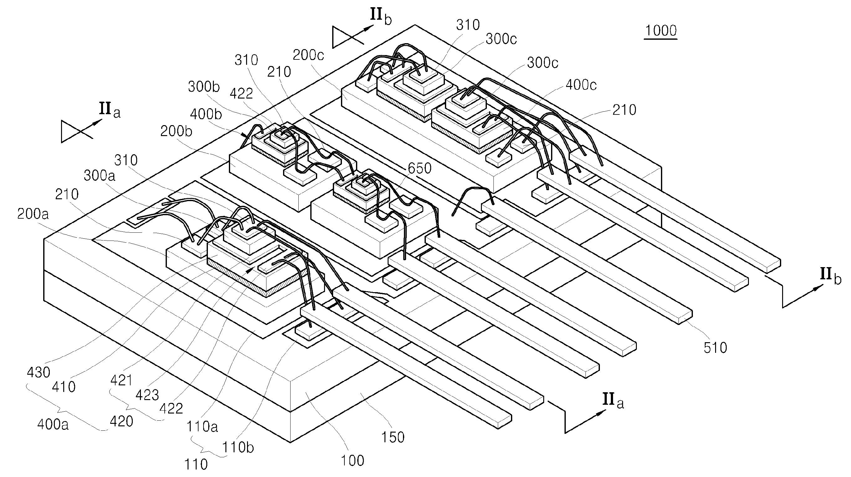
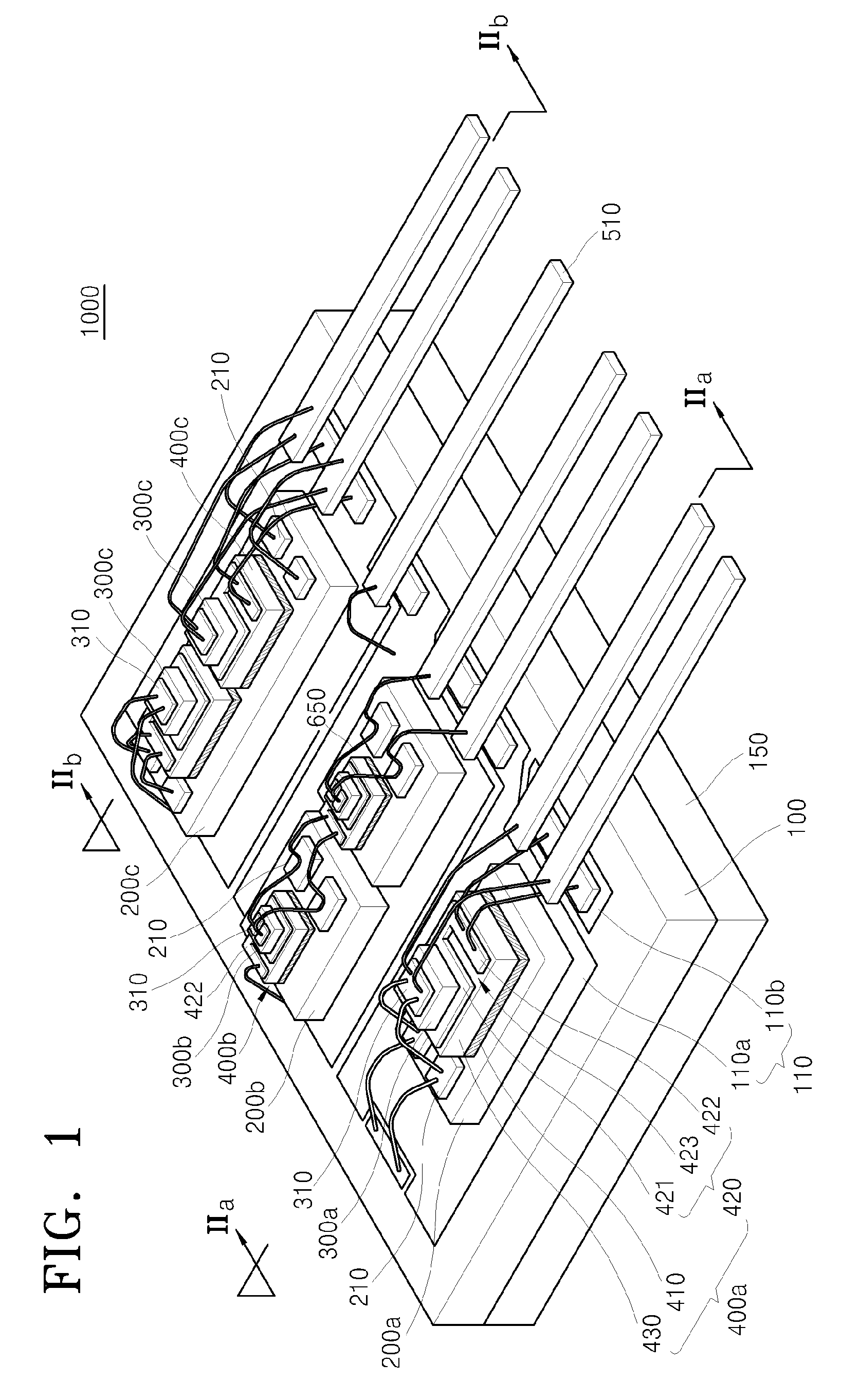
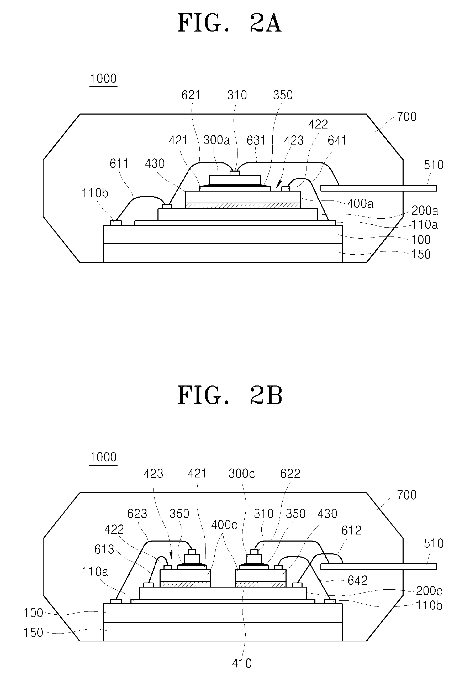
[0024]The present invention will now be described more fully with reference to the accompanying drawings, in which exemplary embodiments according to the invention are shown.

[0025]The invention may, however, be embodied in many different forms and should not be construed as being limited to the embodiments set forth herein; rather, these embodiments are provided so that this disclosure will be thorough and complete, and will fully convey the concept of the invention to those skilled in the art.

[0026]It will also be understood that when a layer is referred to as being “on” another layer or substrate, it can be directly on the other layer or substrate, or intervening layers may also be present. In the drawings, the thicknesses and sizes of layers and regions are exaggerated for clarity, and like reference numerals in the drawings denote like elements. It will also be understood that when an element, such as a layer, a region, or a substrate, is referred to as being “on,”“connected to,...


PUM


Abstract

Provided is a power device package including: a substrate including at least one first die attach region; at least one first power semiconductor chip and at least one second power semiconductor chip that are stacked in order on the first die attach region; at least one die attach paddle that is disposed between the at least one first power semiconductor chip and the at least one second power semiconductor chip, wherein the die attach paddle comprises an adhesive layer that is attached to a top surface of the first power semiconductor chip; a conductive pattern including a second die attach region, on which the second semiconductor chip is mounted, and a wire bonding region that is electrically connected to the second die attach region; and an interlayer member between the adhesive layer and the conductive pattern; and a plurality of firs leads electrically connected to at least one of the at least one first power semiconductor chip and the at least one second power semiconductor chip.

Description

CROSS-REFERENCES TO RELATED APPLICATIONS[0001]This application claims the benefit of Korean Patent Application No. 10-2007-0119309, filed on Nov. 21, 2007 in the Korean Intellectual Property Office, the disclosure of which is incorporated herein in its entirety by reference.BACKGROUND OF THE INVENTION[0002]1. Field of the Invention[0003]The present invention relates to power device packages and methods of manufacturing the same, and more particularly, to power device packages including a plurality of stacked power semiconductor chips, and methods of manufacturing such power device packages.[0004]2. Description of the Related Art[0005]Recent developments in power electronics including such power devices as servo drivers, inverters, silicon-controlled rectifiers (SCRs) and converters are leading to manufacturing light and small power devices with excellent performance characteristics. Related researches are being actively conducted into smart or intelligent power modules in which a va...

Claims


Application Information

Patent Timeline
Patent Type & Authority Applications(United States)
IPC IPC(8): H01L23/495H01L21/60
CPCH01L23/4334H01L2924/1305H01L23/49575H01L24/27H01L24/45H01L24/48H01L24/49H01L24/83H01L24/85H01L2224/274H01L2224/2919H01L2224/32145H01L2224/45015H01L2224/45124H01L2224/45144H01L2224/48091H01L2224/48095H01L2224/48145H01L2224/48227H01L2224/48247H01L2224/484H01L2224/48599H01L2224/48699H01L2224/49H01L2224/73265H01L2224/83101H01L2224/83191H01L2224/83801H01L2224/8385H01L2224/85H01L2224/92H01L2224/92247H01L2924/01005H01L2924/01013H01L2924/01014H01L2924/01028H01L2924/01029H01L2924/01047H01L2924/01079H01L2924/01082H01L2924/014H01L2924/07802H01L2924/0781H01L2924/13055H01L2924/13091H01L2924/14H01L2924/19107H01L2924/20752H01L2924/20753H01L2924/20754H01L2924/20755H01L2924/20756H01L2924/20757H01L2924/00014H01L2924/01006H01L2924/01033H01L2924/0665H01L24/29H01L2224/45139H01L2224/4911H01L2224/49113H01L2924/1306H01L2924/13034H01L23/49562H01L2224/78H01L2924/00H01L2924/181H01L2924/00011H01L2924/2076H01L2924/00012H01L2924/01049H01L2224/85399H01L2224/05599H01L23/12
Inventor JONG, MAN-KYOSON, JOON-SEOLIM, SEUNG-WONJEON, O-SOEB
Owner SEMICON COMPONENTS IND LLC
Why Eureka
Try Eureka