Chip structure, substrate structure, chip package structure and process thereof

Inactive Publication Date: 2009-05-21
ADVANCED SEMICON ENG INC
View PDF4 Cites 9 Cited by
  • Summary
  • Abstract
  • Description
  • Claims
  • Application Information

AI Technical Summary

Benefits of technology

[0008]The present invention is directed to a chip structure, a substrate structure, a chip package structure, and a process of fabricating the chip package structure, so as to remove conventional defects and to improve the reliability of stud bumps.
[0018]In the present invention, the gold-silver alloy containing 5%˜15% of silver by weight is used as the stud bump. Thereby, during a soldering operation, the formation of IMCs and the loss of gold can be prevented since the solder layer is composed of a silver-diffusion constituent.

Problems solved by technology

In addition, after a long time operation, the gold in the stud bumps 110 is diffused to the solder, which may bring about a loss of the gold in the stud bumps 110 or a variation in the composition of the stud bumps 110.

Method used


Image

  • Chip structure, substrate structure, chip package structure and process thereof
  • Chip structure, substrate structure, chip package structure and process thereof
  • Chip structure, substrate structure, chip package structure and process thereof

Examples


first embodiment

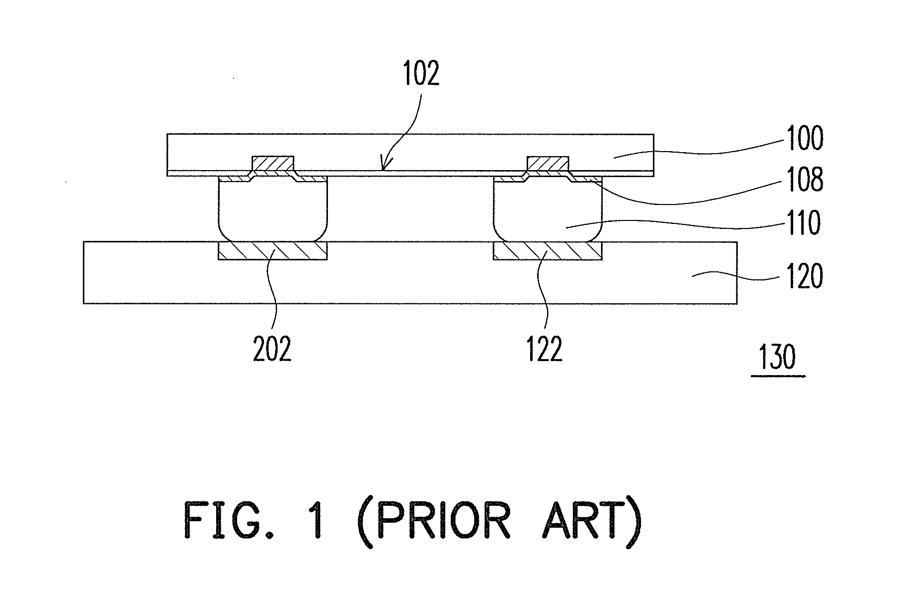
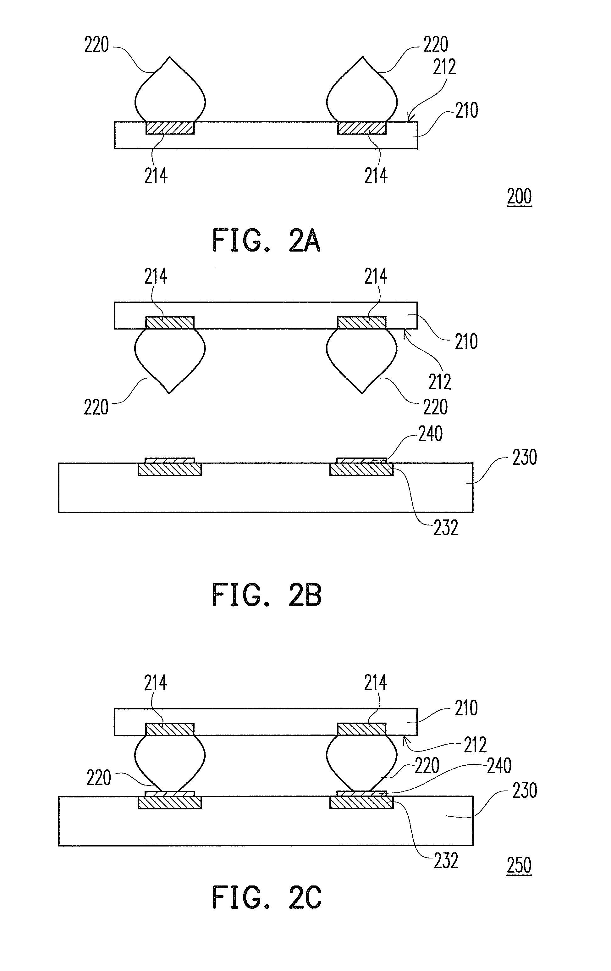
[0026]FIGS. 2A through 2C are schematic views of a chip package structure and a process of fabricating the same according to the present invention. Referring to FIG. 2A, a chip package structure 200 includes a chip 210 and a plurality of stud bumps 220. A plurality of bonding pads 214 are disposed on an active surface 212 of the chip 210, and the bonding pads 214 are, for example, made of aluminumn. Here, the bonding pads 214 serve as input / output interfaces of electronic signals. The chip 210 can be used in ball grid array (BGA) structures, such as semiconductor devices including light sensing devices, light emitting devices, or processors. The stud bumps 220 are bump-shaped gold balls formed by melting gold wires with use of a wire-bonding machine. After the gold balls are pressed onto the bonding pads 214, the gold wires are cut off. The use of the gold bumps formed by wire bonding and EFO is conducive to accelerating the manufacturing process and improving throughput, so as to e...

second embodiment

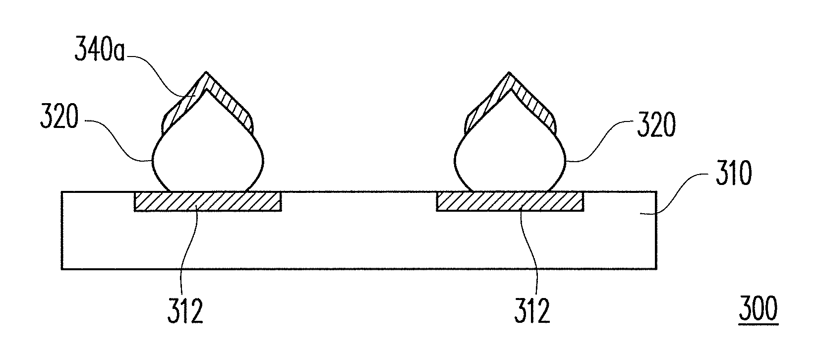
[0030]FIGS. 3A through 3C are schematic views of a chip package structure and a process of fabricating the same according to the present invention. Referring to FIG. 3A, a chip package structure 300 includes a substrate 310 and a plurality of stud bumps 320. The substrate 310 is, for example, a printed circuit board, and the substrate 310 has a plurality of contact pads 312 made of copper, for example. The stud bumps 320 are bump-shaped gold balls formed by melting gold wires with use of a wire-bonding machine. After the gold balls are pressed onto the bonding pads 312, the gold wires are cut off. The formation of the stud bumps 320 on the substrate 310 can prevent the wire-bonding machine from exerting an excessive strength to the chip. As such, integrated circuits within the chip are not damaged. Additionally, it is more cost-effective to fabricate the stud bumps 320 on the substrate 310. Besides, the yield and the throughput can be improved while the rework rate can be reduced.

[0...


PUM

PropertyMeasurementUnit
Percent by massaaaaaaaaaa

Abstract

A chip package structure and process are provided; the structure includes a substrate, a chip, a solder layer and at least a stud bump. The substrate has at least a contact pad, and the chip has an active surface where at least a bonding pad is disposed. The stud bump is disposed on the bonding pad of the chip or on the contact pad of the substrate, and the stud bump joints with the solder layer to fix the chip on the substrate. The stud bump is made of gold-silver alloy containing silver below 15% by weight.

Description

CROSS-REFERENCE TO RELATED APPLICATION[0001]This application claims the priority benefit of Taiwan application serial no. 96143775, filed Nov. 19, 2007. The entirety of the above-mentioned patent application is hereby incorporated by reference herein and made a part of this specification.BACKGROUND OF THE INVENTION[0002]1. Field of the Invention[0003]The present invention relates to a semiconductor package structure, and more particularly, to a chip structure, a substrate structure, a chip package structure, and a process of fabricating the chip package structure.[0004]2. Description of Related Art[0005]In the current era, a semiconductor industry is characterized by high integration and great maturity of technology. To comply with diverse market demands, various chip package structures including optoelectronic products, light emitting devices, and light sensing devices (image sensors) are developed and manufactured by performing a process for fabricating semiconductors, thus giving...

Claims


Application Information

Patent Timeline
IPC IPC(8): H01L23/498
CPCB23K35/0233H01L2224/0401B23K35/22B23K35/3013C22C5/02H01L23/49811H01L24/12H01L24/16H01L24/81H01L2224/1134H01L2224/13099H01L2224/13144H01L2224/812H01L2224/81205H01L2224/81801H01L2924/01013H01L2924/01029H01L2924/01033H01L2924/01046H01L2924/01079H01L2924/01082H01L2924/01322H01L2924/01327H01L2924/14H01L2224/0558H01L2224/05624H01L2924/01006H01L2924/01047B23K35/0244H01L2924/00013H01L2224/29099H01L24/13H01L2224/81191H01L2224/81192H01L2924/00014
Inventor SHEN, CHI-CHIHCHEN, JEN-CHUANCHANG, HUI-SHANPAN, TOMMY
Owner ADVANCED SEMICON ENG INC
Why Eureka
Try Eureka