Power supply controller and semiconductor device

a technology of power supply controller and semiconductor device, which is applied in the direction of process and machine control, pulse technique, instruments, etc., can solve the problems of reducing the accuracy of anomaly detection, the characteristics of the elements used for current detection or threshold setup vary, etc., and achieves the effect of rapid protection

Active Publication Date: 2009-05-21
AUTONETWORKS TECH LTD +2
View PDF1 Cites 28 Cited by
  • Summary
  • Abstract
  • Description
  • Claims
  • Application Information

AI Technical Summary

Benefits of technology

[0007]In the power supply controller of the present invention, the threshold current can be set so as to increase or decrease with increase or decrease of the output-side voltage (e.g., the source voltage in the case of an N-channel MOSFET, or the drain voltage in the case of a P-channel MOSFET) of the semiconductor switching element. Thereby, in case that short-circuiting occurs in the load, for example, the level of a load current will immediately reach the threshold current level, so that rapid protection can be achieved compared to a construction in which a threshold is set to a constant level.

Problems solved by technology

In the case that an overcurrent detecting function is provided in such a semiconductor device, the problem arises that the elements used for current detection or threshold setup have variation in characteristics.
That is, in the case that an anomaly is detected by comparing an overcurrent, detected using a shunt resistor, a sense FET or the like, with a predetermined threshold, precise setup of the threshold cannot be achieved due to manufacturing variation resulting in reduction of the precision of anomaly detection, if the resistor for threshold setup is disposed within the semiconductor device.

Method used


Image

  • Power supply controller and semiconductor device
  • Power supply controller and semiconductor device
  • Power supply controller and semiconductor device

Examples


first embodiment

[0037]A first embodiment according to the present invention will be explained with reference to FIGS. 1 to 3 and 5.

[0038](1) General Construction

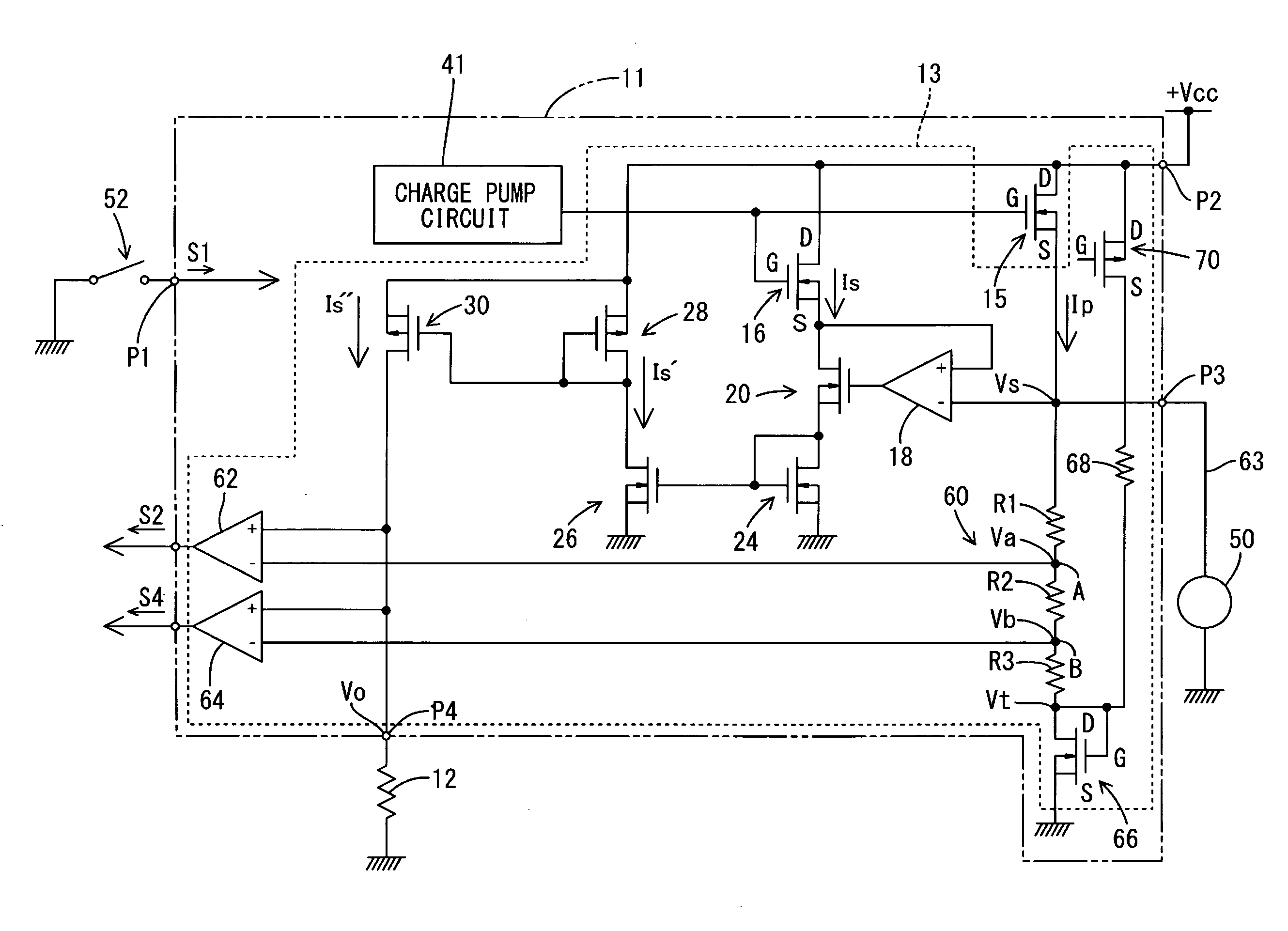
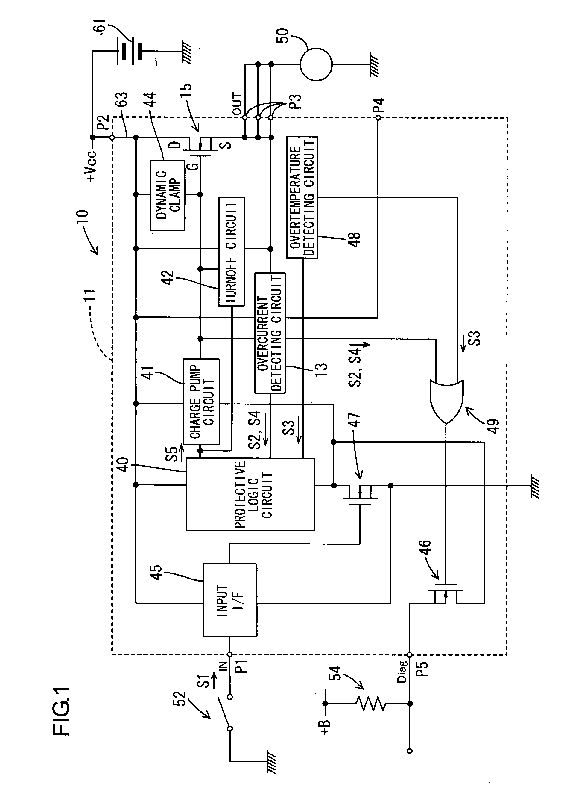
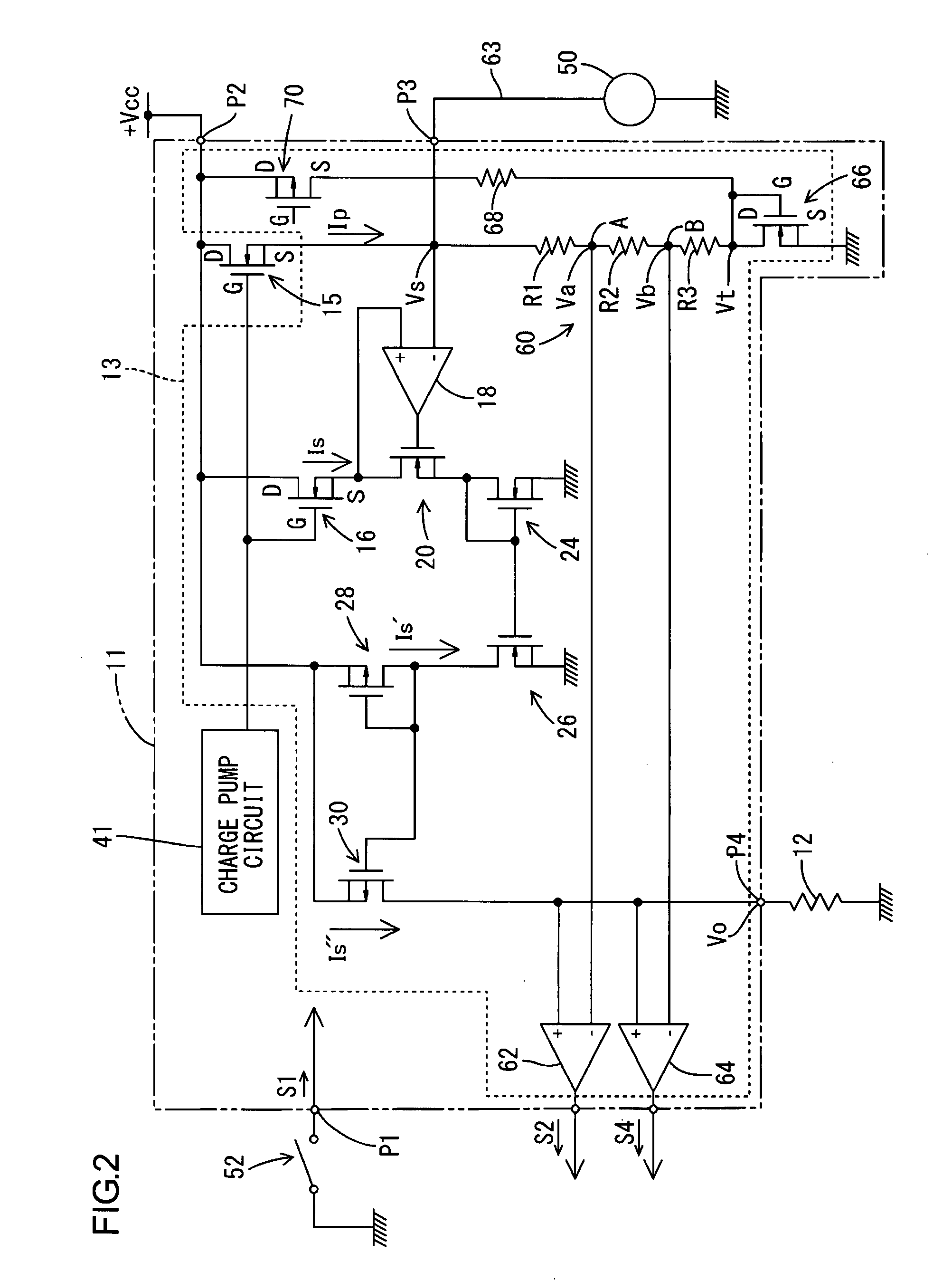
[0039]FIG. 1 is a block diagram showing the general construction of a power supply controller 10 according to the present embodiment. As shown in the figure, the power supply controller 10 of the present embodiment includes a power MOSFET 15 (i.e., an example of “a semiconductor switching element” and “a power FET” of the present invention) disposed on a current supply line 63 connected between a power source 61 (a vehicle power source) and a load 50, so as to control the power supply from the power source 61 to the load 50 by switching the power MOSFET 15 between ON and OFF. In the present embodiment, the power supply controller 10 can be installed on a vehicle not shown, and used for drive control for the load 50 such as a vehicle lamp, a cooling fan motor or a defogger heater.

[0040]As shown in FIG. 1, the power supply controller 10 is fo...

second embodiment

[0066]FIG. 4 shows a second embodiment. The difference from the first embodiment is in the construction of a bias circuit. The other constructions are similar to the first embodiment, and therefore designated by the same symbols as the first embodiment. Redundant explanations are omitted, and the following explanation will be concentrated on the difference.

[0067]As shown in FIG. 4, according to the present embodiment, the bias circuit is disposed on the upstream-end side of the voltage-dividing circuit 60, i.e., between the power supply terminal P2 and the voltage-dividing circuit 60. Specifically, the downstream end of the above-described bias resistor 68 is connected to the connecting point between the source S of the power MOSFET 15 and the voltage-dividing resistor R1.

[0068]According to this construction, when a low-level control signal S1 is inputted to the input terminal P1, the FET 70 turns on, i.e., turns to a conductive state, so as to permit conduction between the power su...


PUM


Abstract

A voltage-dividing circuit 60, which is formed of serially connected voltage-dividing resistors R1, R2, R3, is disposed between the source terminal S of a power MOSFET 15 and the ground. The divided voltage Va at a connecting point A is applied to one of the input terminals of a comparator 62, while the divided voltage Vb at a connecting point B is applied to one of the input terminals of a comparator 64. The other input terminals of the comparators 62, 64 are connected to the connecting line between an external terminal P4, to which an external resistor 12 is connected, and an FET 30.

Description

TECHNICAL FIELD[0001]The present invention relates to a power supply controller and a semiconductor device.BACKGROUND ART[0002]A power supply controller is conventionally provided, in which a high-power semiconductor switching element such as a power MOSFET is disposed on a current supply line connected between a power source and a load, and which is configured to control the power supply to the load by switching the semiconductor switching element between ON and OFF. In such a power supply controller, it is known that a self-protective function is provided for protecting its own semiconductor switching element. The self-protective function turns off the semiconductor switching element by controlling the potential of the control terminal (e.g., the gate in the case of a MOSFET) of the semiconductor switching element, when an overcurrent (i.e., an abnormal current) has occurred due to short-circuiting in the load, for example. Specifically, as shown in JP-A-2001-217696, for example, ...

Claims


Application Information

Patent Timeline
Patent Type & Authority Applications(United States)
IPC IPC(8): G05F1/573
CPCG05F1/575H03K17/0822H03K17/063H03K2217/0027
Inventor TAKAHASHI, SEIJIKATO, MASAYUKIFURUICHI, MASAHIKOISSHIKI, ISAO
Owner AUTONETWORKS TECH LTD
Why Eureka
Try Eureka