Intrinsic amorphous silicon layer

a silicon layer and amorphous silicon technology, applied in the field can solve the problems of low efficiency, high cost, and low efficiency of thin film solar cells

Inactive Publication Date:
View PDF103 Cites 12 Cited by
  • Summary
  • Abstract
  • Description
  • Claims
  • Application Information

AI Technical Summary

Benefits of technology

[0008]Embodiments of the present invention may further provide a method of forming a p-i-n junction over a substrate, comprising depositing a p-doped silicon layer over a surface of a substrate, depositing an n-doped silicon layer over the surface of the substrate, depositing an intrinsic amorphous silicon layer between the p-doped silicon layer and the n-doped silicon layer, depositing a first intrinsic microcrystalline silicon layer on the intrinsic amorphous silicon layer by providing hydrogen gas and silane gas at a ratio of greater than about 200:1, and depositing a second intrinsic microcrystalline silicon layer on the first intrinsic microcrystalline silicon layer by providing hydrogen gas and silane gas at a ratio of less than about 200:1.
[0009]Embodiments of the present invention may further provide a method of forming a p-i-n junction over a substrate, comprising depositing a p-doped silicon layer over a surface of the substrate in a first process chamber disposed within a first processing system, transferring the substrate from the first process chamber to a second process chamber which is disposed within the first processing system, wherein transferring the substrate is performed in a vacuum environment, and depositing two or more layers over the surface of the p-doped silicon layer while the substrate is positioned in the second process chamber, comprising depositing an intrinsic amorphous silicon layer on the p-doped silicon layer, depositing an intrinsic microcrystalline silicon layer on the intrinsic amorphous silicon layer, and depositing an n-doped silicon layer on the intrinsic microcrystalline silicon layer.

Problems solved by technology

Problems with current thin film solar cells include low efficiency and high cost.

Method used


Image

  • Intrinsic amorphous silicon layer
  • Intrinsic amorphous silicon layer
  • Intrinsic amorphous silicon layer

Examples


Embodiment Construction

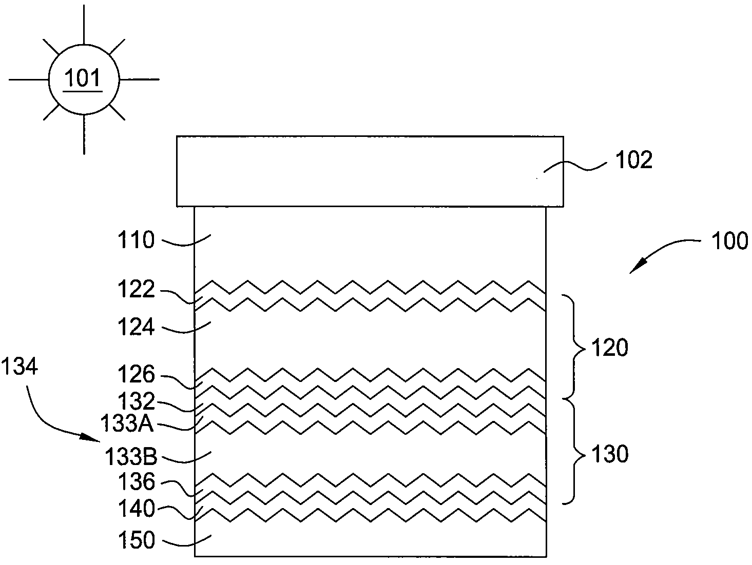
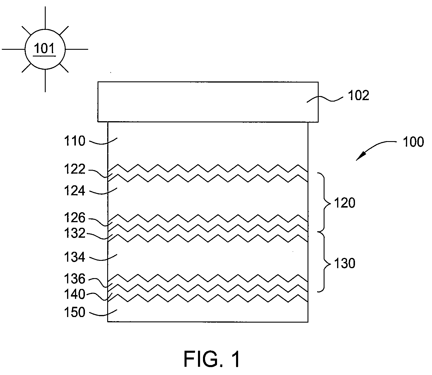
[0018]Embodiments of the present invention include improved thin film solar cells and methods and apparatus for forming the same. For ease and clarity of description, the present invention will be described in reference to the tandem junction solar cell of FIG. 1, although, the present invention may be used to advantage to form other single junction, tandem junction, or multi-junction solar cells.

[0019]FIG. 1 is a schematic diagram of a multi-junction solar cell 100 oriented toward the light or solar radiation 101. Solar cell 100 comprises a substrate 102, such as a glass substrate, polymer substrate, or other suitable transparent substrate, with thin films formed thereover. The solar cell 100 further comprises a first transparent conducting oxide (TCO) layer 110 formed over the substrate 102, a first p-i-n junction 120 formed over the first TCO layer 110, a second p-i-n junction 130 formed over the first p-i-n junction 120, a second TCO layer 140 formed over the second p-i-n juncti...


PUM

PropertyMeasurementUnit
frequencyaaaaaaaaaa
frequencyaaaaaaaaaa
frequencyaaaaaaaaaa

Abstract

Embodiments of the present invention may include an improved thin film solar cell device that is formed by sequentially depositing an intrinsic amorphous silicon layer and an intrinsic microcrystalline silicon layer during the p-i-n or n-i-p junction formation process. Embodiments of the invention also generally provide a method and apparatus for forming the same. The present invention may be used to advantage to form other single junction, tandem junction, or multi-junction thin film solar cell devices.

Description

CROSS-REFERENCE TO RELATED APPLICATIONS[0001]This application claims benefit of U.S. Provisional Patent Application Ser. No. 60 / 985,195, filed Nov. 2, 2007, and entitled “Intrinsic Amorphous Silicon Layer,” which is herein incorporated by reference.BACKGROUND OF THE INVENTION[0002]1. Field of the Invention[0003]Embodiments of the present invention generally relate to solar cells and methods and apparatuses for forming the same. More particularly, embodiments of the present invention relate to thin film solar cells and methods and apparatuses for forming the same.[0004]2. Description of the Related Art[0005]Crystalline silicon solar cells and thin film solar cells are two types of solar cells. Crystalline silicon solar cells typically use either mono-crystalline substrates (i.e., single-crystal substrates of pure silicon) or a multi-crystalline silicon substrates (i.e., poly-crystalline or polysilicon). Additional film layers are deposited onto the silicon substrates to improve light...

Claims


Application Information

Patent Timeline
Patent Type & Authority Applications(United States)
IPC IPC(8): H01L21/20H01L31/075
CPCC23C16/24C23C16/4405C23C16/5096H01J37/32091H01J37/32357H01J2237/3321Y02E10/548H01L31/076H01L31/1824H01L31/202H01L31/206Y02E10/545H01L31/075Y02P70/50
Inventor CHOI, SOO YOUNGCHAE, YONG-KEESHENG, SHURANLI, LIWEI
Why Eureka
Try Eureka