Method of forming a multifilament ac tolerant conductor with striated stabilizer, articles related to the same, and devices incorporating the same

a technology of striated stabilizer and conductor, which is applied in the field of high temperature superconductors, can solve the problems of many challenges, high energy cost and end-use consumption in the united states, and the fabrication of commercially feasible hts tap

Active Publication Date: 2009-05-21
SUPERPOWER INC
View PDF21 Cites 42 Cited by
  • Summary
  • Abstract
  • Description
  • Claims
  • Application Information

AI Technical Summary

Problems solved by technology

Energy costs and end-use consumption in the United States has risen dramatically over the past few years.
However, many challenges exist with the commercialization of HTS superconductors.
In particular, one obstacle has been the fabrication of a commercially feasible HTS tape that can be used to form the various power components.
Due to materials and manufacturing costs, however, such tapes do not represent a commercially feasible product for the extended lengths need.
The architecture of the coated conductor has not been optimized for AC applications, however, such as motors, generators, and transformers.
In particular, the width and thickness of HTS tapes have a high dimension ratio, which in turn results in HTS coated conductors exhibiting very high hysteretic losses.
Although these multifilament conductors have been shown to greatly reduce hysteretic losses, numerous engineering and manufacturing challenges remain prior to full commercialization of striated second generation-tapes.
Forming striations through the thick stabilizer layer using known chemical-etching techniques is prohibitively laborious, such that the fabrication of a multifilament HTS tape with a thick stabilizer layer has not yet been possible.
In particular, etching through a thick stabilizer layer in addition to the thin capping layer, before reaching the HTS layer, results in much longer period of contact with a particular etching agent.
A longer etching contact time causes an increase in the degradation of the HTS materials and a loss of superconducting properties due to an increased chemical reaction.
Accordingly, it has not been feasible to use state of the art etching techniques in order to form multifilament HTS tapes with thick stabilizers.

Method used


Image

  • Method of forming a multifilament ac tolerant conductor with striated stabilizer, articles related to the same, and devices incorporating the same
  • Method of forming a multifilament ac tolerant conductor with striated stabilizer, articles related to the same, and devices incorporating the same
  • Method of forming a multifilament ac tolerant conductor with striated stabilizer, articles related to the same, and devices incorporating the same

Examples


example 1

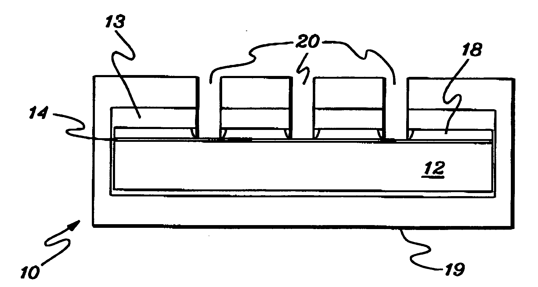
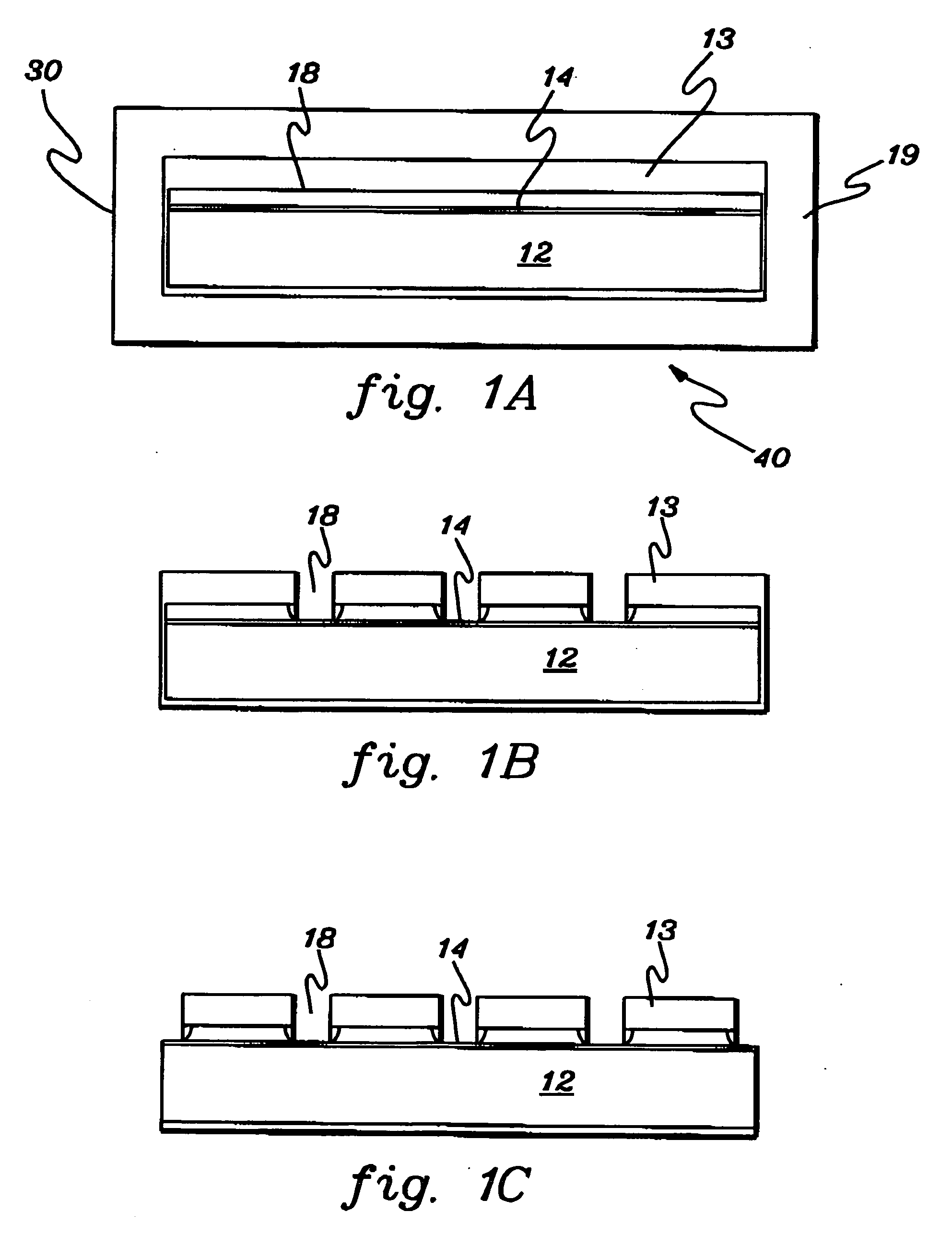
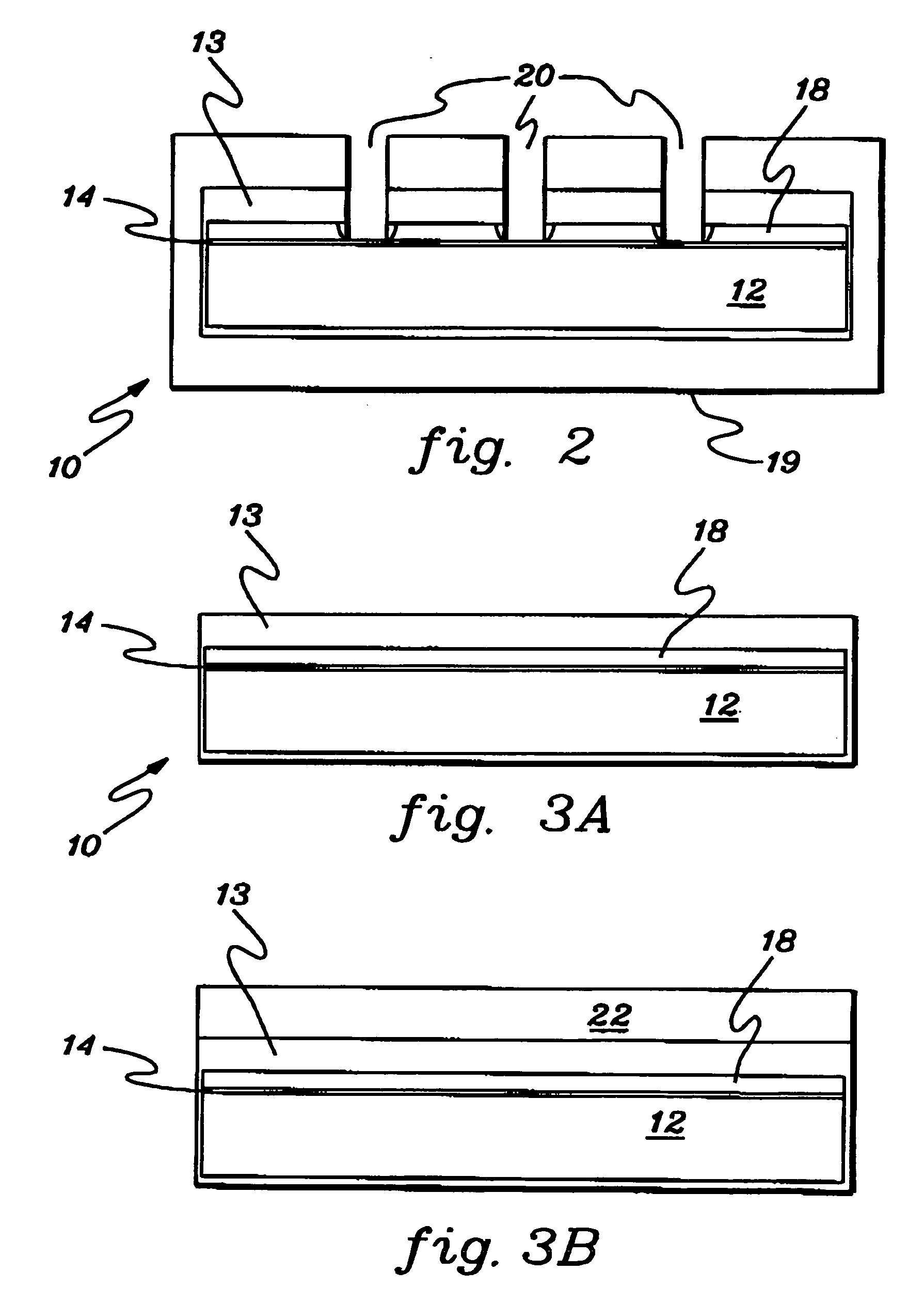
[0066]Samples were created utilizing the novel striation technique described above. In particular, samples were provided using 4 mm width of substrate with a thickness of 50 microns. In these particular samples, the substrate used was a nickel-based alloy (Hastelloy C276). A buffer layer stack comprising of alumina, yttria, MgO, and LaMnO3 were deposited to a total thickness of 160 nm. Next, MOCVD (Metalorganic Chemical Vapor Deposition) process was performed to form a one micron thick YBCO layer. Next, samples were then subjected to magnetron sputtering of silver to form 3-micron thick capping layers. Next, a layer of dry film photoresist was coated, such that a known photolithographic technique, i.e. broad band UV exposure and photoresist developing, could be used to transfer the desired striation pattern. Those samples were placed in a copper-sulfate solution and biased such that the capping layers formed a cathode, the anode being a copper plate. Electroplating was carried out t...

example 2

[0067]Samples were created utilizing the novel striation technique described above. In particular, samples were provided using 4 mm width of substrate with a thickness of 50 microns. In these particular samples, the substrate used was a nickel-based alloy (Hastelloy C276). A buffer layer stack comprising of alumina, yttria, MgO, and LaMnO3 were deposited to a total thickness of 160 nm. Next, MOCVD (Metalorganic Chemical Vapor Deposition) process was performed to form a one-micron thick YBCO layer. Next, samples were then subjected to magnetron sputtering of silver to form 3-micron thick capping layers. Next, a polyimide film was laminated, such that a known laser ablation technique, i.e. using 308 nm or 248 nm excimer laser, could be used to transfer the desired striation pattern in a single step. Those samples were placed in a copper-sulfate solution and biased such that the capping layers formed a cathode, the anode being a copper plate. Electroplating was carried out to form a co...

example 3

[0068]Samples were created utilizing the novel striation technique described above. In particular, samples were provided using 4 mm width of substrate with a thickness of 50 microns. In these particular samples, the substrate used was a nickel-based alloy (Hastelloy C276). A buffer layer stack comprising of alumina, yttria, MgO, and LaMnO3 were deposited to a total thickness of 160 nm. Next, MOCVD (Metalorganic Chemical Vapor Deposition) process was performed to form a one-micron thick YBCO layer. Next, a 30-micron thick layer of dry film photoresist was coated, such that a known photolithographic technique, i.e. broad band UV exposure and photoresist developing, could be used to transfer the desired striation pattern. Then, samples were subjected to physical vapor deposition process to coat a 1-micron thick capping layer such as copper. In this deposition process such as metal evaporation, temperature is controlled to be compatible with photoresist remaining on samples. Next, those...


PUM

PropertyMeasurementUnit
thicknessaaaaaaaaaa
critical temperature Tcaaaaaaaaaa
thicknessaaaaaaaaaa

Abstract

A multifilament high temperature superconductor with thick, striated stabilizer is disclosed, including a substrate, a buffer layer, a multifilament superconductor layer, and at least one thick stabilizer layer. Also disclosed are components incorporating superconducting tapes and methods for manufacturing same.

Description

STATEMENT REGARDING FEDERALLY SPONSORED RESEARCH OR DEVELOPMENT[0001]This invention is the result of a contract with the United States Air Force Research Laboratory, under contract no. FA865004-C-2476.FIELD OF THE INVENTION[0002]The present invention relates generally to high temperature superconductors (HTS), and more specifically a novel method for forming a multifilament AC tolerant superconductor with a thick, striated stabilizer, and articles manufactured using the method.BACKGROUND[0003]Energy costs and end-use consumption in the United States has risen dramatically over the past few years. Electricity, which accounts for almost half of the end-use energy consumption in the US, is highly dependent on the price of fossil fuels. With the rising demand and cost comes a requirement for more efficient and cost effective power and, in order to reduce dependence on fossil fuels, improvements in energy efficiency are needed.[0004]Superconductor materials have been known and understood...

Claims


Application Information

Patent Timeline
Patent Type & Authority Applications(United States)
IPC IPC(8): H01L39/02H01L39/24
CPCH01L39/143H01L39/248Y10T428/265Y10T29/49014Y10S428/933H10N60/203H10N60/0801Y02E40/60H10N60/01
Inventor ZHANG, XUNSELVAMANICKAM, VENKAT
Owner SUPERPOWER INC
Why Eureka
Try Eureka