Method for forming conductive pattern and wiring board

a conductive pattern and wiring board technology, applied in the direction of resistive material coating, solid-state device coating, chemical vapor deposition coating, etc., can solve the problems of time and labor for forming a conductive pattern in general, and achieve the effect of stable structure and easy formation

Active Publication Date: 2009-05-28
PANASONIC CORP
View PDF4 Cites 9 Cited by
  • Summary
  • Abstract
  • Description
  • Claims
  • Application Information

AI Technical Summary

Benefits of technology

[0030]In the conductive pattern formation method of this invention, gas bubbles are generated from a gas bubble generating agent included in a fluid body by heating the fluid body supplied into a gap between a substrate and a flat plate, and the fluid body is forced out of the gas bubbles by the growing gas bubbles, so that the fluid body can be allowed to self-assemble between a convex pattern formed on the flat plate and the substrate owing to the interfacial force. As a result, an aggregate of the conductive particles included in the fluid body having self-assembled forms a condu

Problems solved by technology

In the case where a conductive pattern (a wiring pattern) is formed on a substrate such as a printed board, photolithography and etching are performed in ge

Method used


Image

  • Method for forming conductive pattern and wiring board
  • Method for forming conductive pattern and wiring board
  • Method for forming conductive pattern and wiring board

Examples


Embodiment Construction

[0055]The present inventor has made various examinations on a method for forming a bump through self-assembly of conductive particles (such as a solder powder) on an electrode of a wiring board or a semiconductor chip, or on a flip-chip mounting method by forming a connecting body between electrodes of a wiring body and a semiconductor chip through self-assembly of conductive particles between the electrodes, and has proposed a novel bump formation method and a novel flip-chip mounting method (Japanese Patent Application No. 2005-094232).

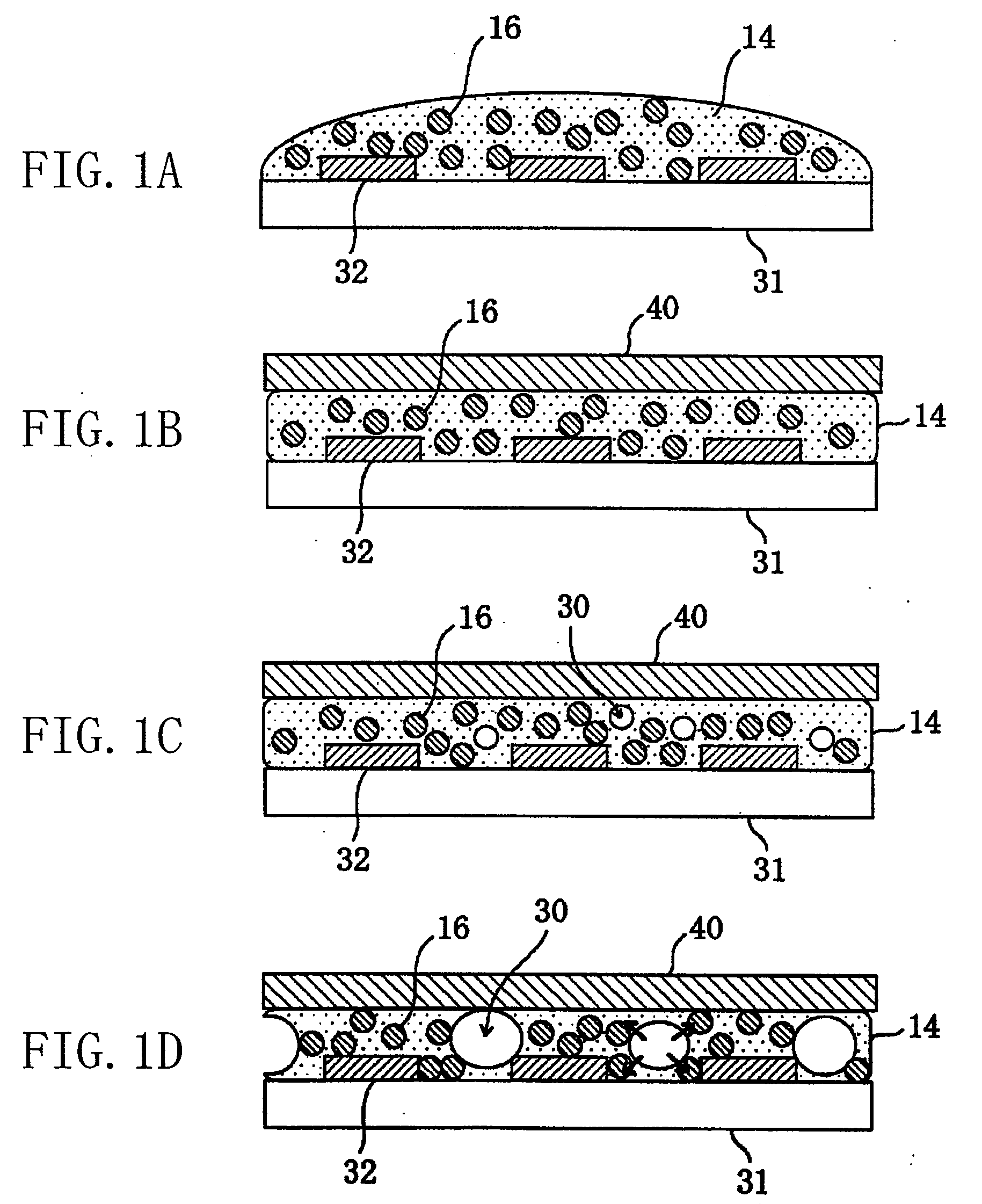
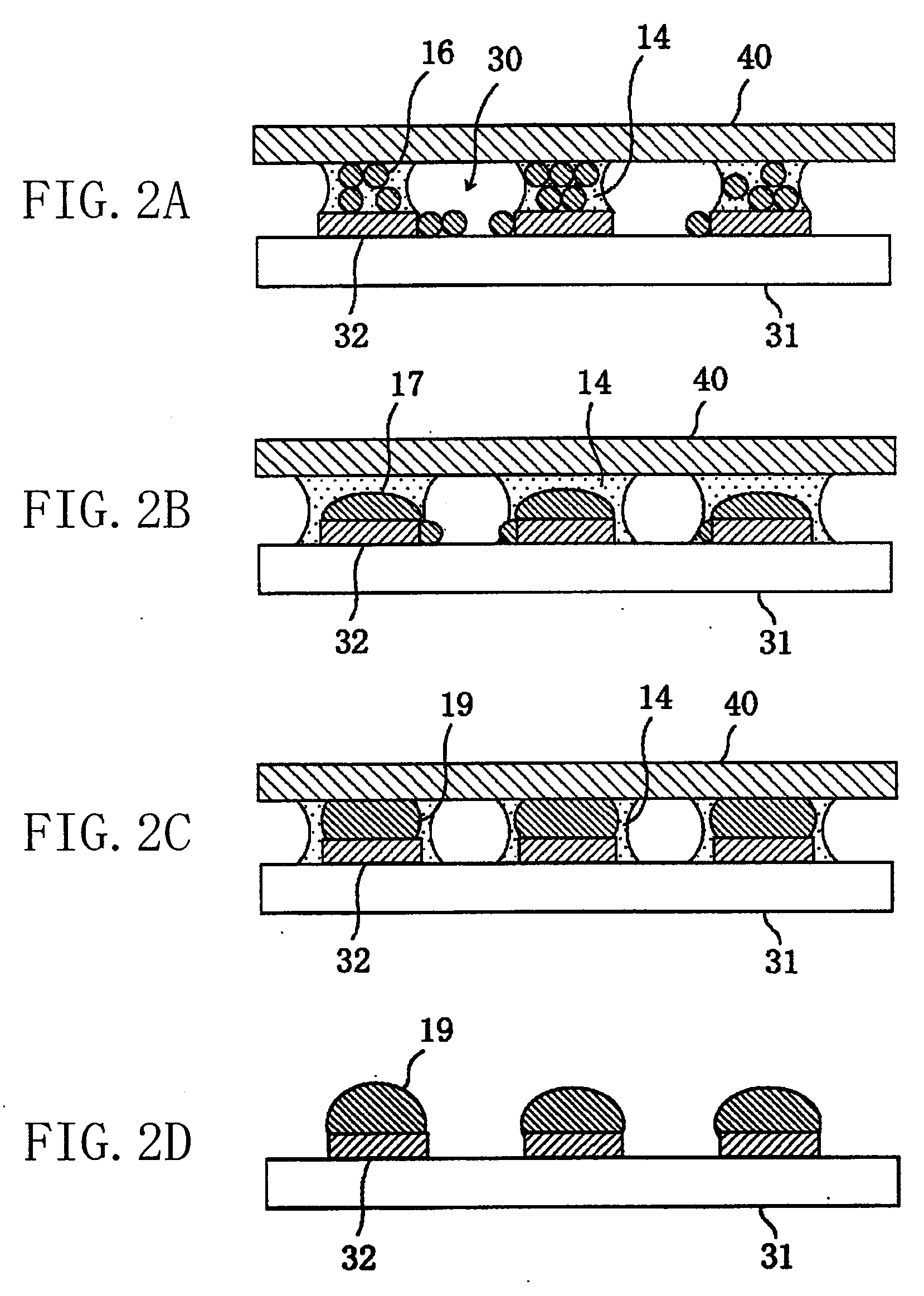
[0056]FIGS. 1A through 1D and 2A through 2D are diagrams for showing basic procedures in the bump formation method disclosed by the present inventor in the aforementioned patent application. The bump formation method alone will be herein described because the basic procedures are common to the flip-chip mounting method.

[0057]First, as shown in FIG. 1A, a fluid body (resin) 14 including conductive particles (solder powder) 16 and a gas bubble generat...


PUM

PropertyMeasurementUnit
Temperatureaaaaaaaaaa
Forceaaaaaaaaaa
Electrical conductoraaaaaaaaaa

Abstract

[Summary]
[Problem] To provide a conductive pattern formation method in which a fine pattern can be formed in a simple way at low cost.
[Means for solving problem] A flat plate having a convex pattern on its surface is provided so as to oppose a substrate, a fluid body including conductive particles and a gas bubble generating agent is supplied into a gap between the substrate and the flat plate, and thereafter, the fluid body is heated for generating gas bubbles from the gas bubble generating agent included in the fluid body. The fluid body is forced out of the gas bubbles as the gas bubbles generated from the gas bubble generating agent grow, so as to self-assemble between the convex pattern formed on the flat plate and the substrate owing to interfacial force, and an aggregate of the conductive particles included in the fluid body having self-assembled is made into a conductive pattern formed on the substrate.

Description

TECHNICAL FIELD[0001]The present invention relates to a method for forming a conductive pattern on a substrate, and more particularly, it relates to a method for forming a conductive pattern in which a fine pattern can be obtained in a simple way.BACKGROUND ART[0002]In the case where a conductive pattern (a wiring pattern) is formed on a substrate such as a printed board, photolithography and etching are performed in general, and since these processes include a large number of complicated procedures, time and labor are necessary for forming a conductive pattern in general.[0003]As a technique to form a fine conductive pattern without performing such processes, a method in which a conductive pattern is drawn on a substrate by using a conductive paste including metal nano-particles and the thus obtained conductive paste layer is heated for forming a desired conductive pattern is known (for example, Patent Documents 1, 2 and the like).[0004]As a general method for drawing a conductive ...

Claims


Application Information

Patent Timeline
IPC IPC(8): H05K1/00B05D5/12B05D3/06
CPCH01L21/4846H05K3/04H05K3/101H05K3/102H05K3/3484Y10T156/1744H05K2203/0425H05K2203/083H05K2203/087Y10T29/49155H05K2203/0108H01L2224/11H05K3/3485
Inventor KARASHIMA, SEIJIKITAE, TAKASHINAKATANI, SEIICHI
Owner PANASONIC CORP
Why Eureka
Try Eureka