

Production method of multilayer printed wiring board and multilayer printed wiring board
a multi-layer printing and wiring board technology, applied in the direction of printed element electric connection formation, cable/conductor manufacturing, conductive pattern formation, etc., can solve the problems of deteriorating flow of plating solution, reducing insulation reliability, and etching back phenomenon in such via holes, so as to reduce the length of the protruding glass cloth, the effect of reducing flowability and high reliability
- Summary
- Abstract
- Description
- Claims
- Application Information
AI Technical Summary
Benefits of technology
Problems solved by technology
Method used
Image

Examples
example 1
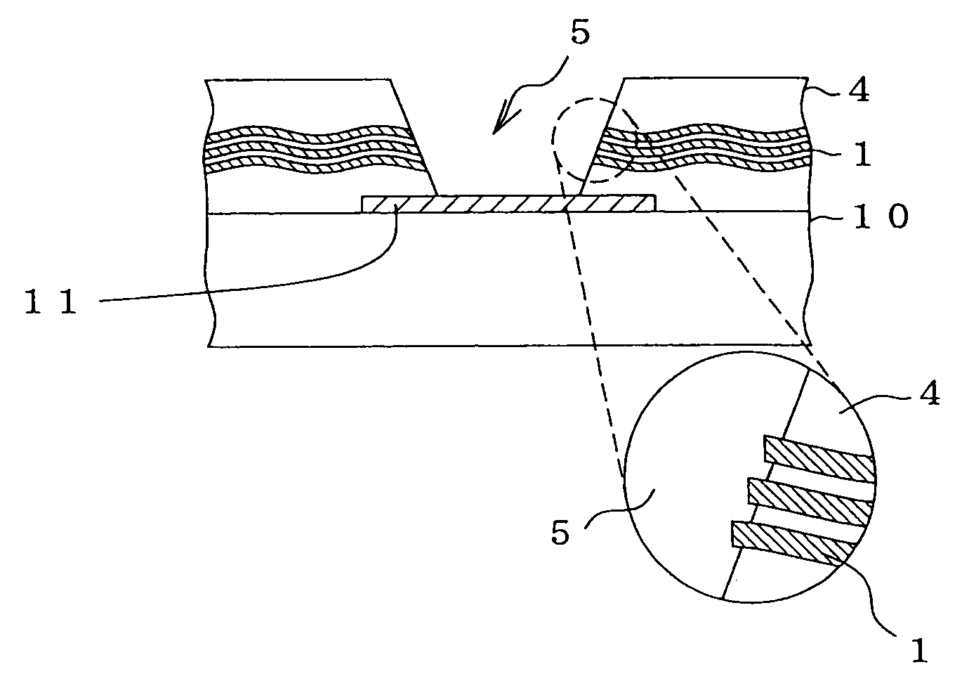
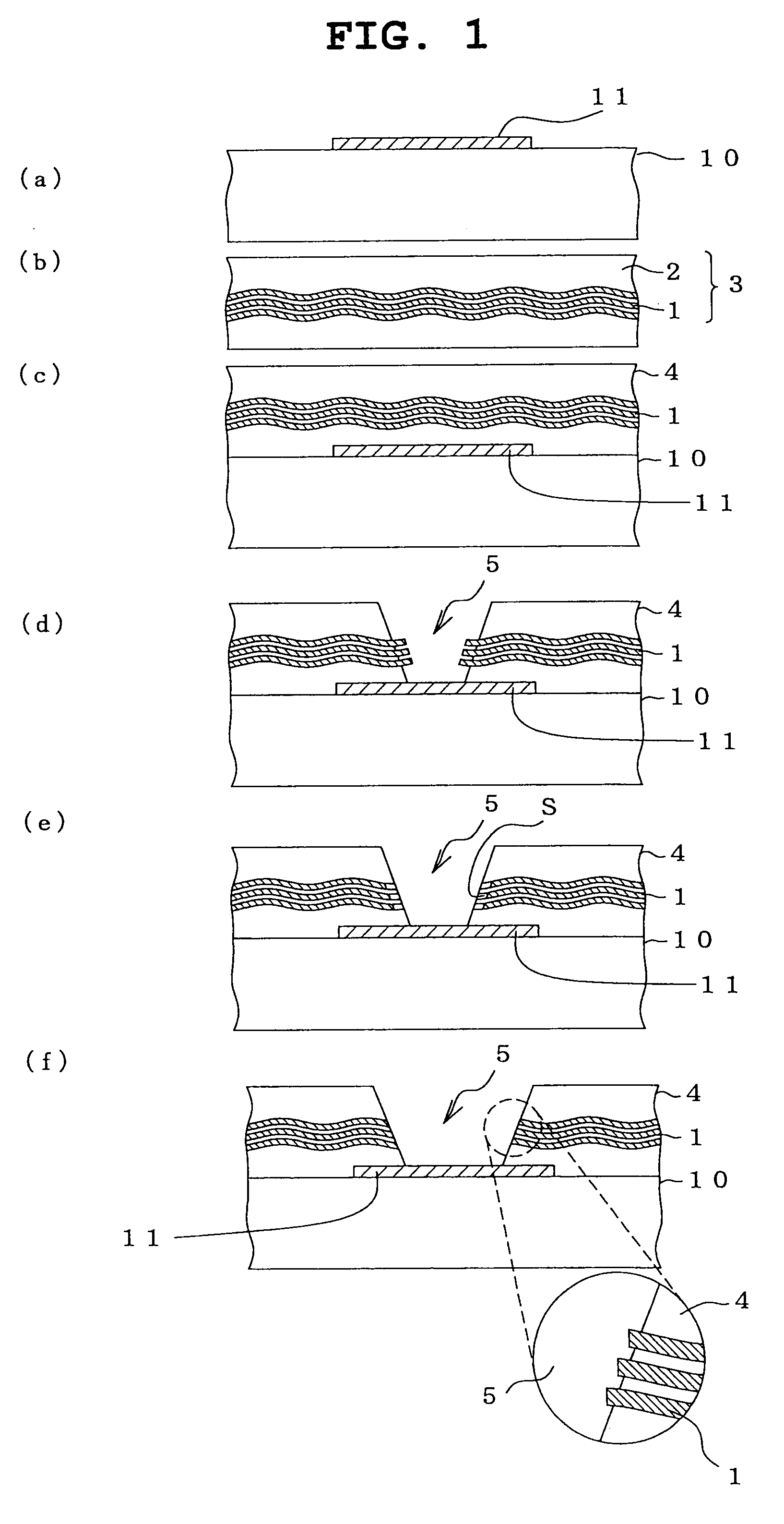
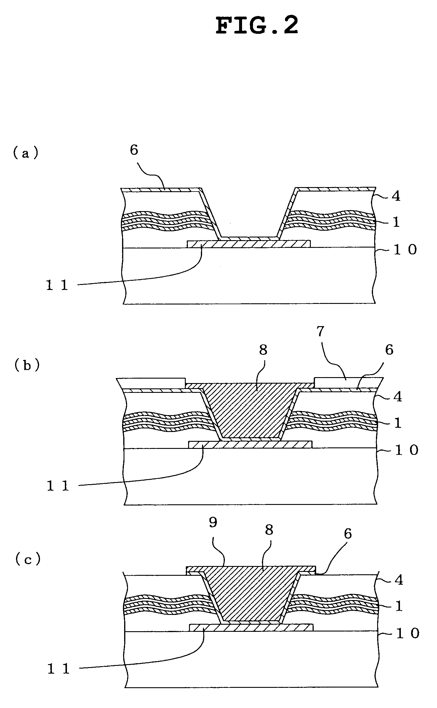
[0092]A protection film-detached prepreg with PET film was laminated on both sides of a copper-clad laminate plate (circuit substrate) having a thickness of 0.2 mm after circuit formation (circuit conductor thickness 18 μm). The PET film was detached, and the laminate was thermally cured to form an insulating layer having a thickness of 32 μm on both surfaces of the above-mentioned circuit substrate. Then, a via hole having a top diameter 60 μm, a bottom diameter 50 μm was formed in the insulating layer laminated on one surface of the circuit substrate by carbon dioxide gas laser.
[0093]The resulting circuit substrate was immersed in an aqueous solution, which was obtained by diluting a glass etching solution (“Enplate MLB GLASS ETCH ADDITIVE” manufactured by Meltex Inc.) containing fluoroboric acid at a concentration of about 50 g / L with ion exchange water to a concentration of 20 mL / L, at 40° C. for 5 minutes for etching of the glass cloth. Then the via hole was subjected to a desm...
example 2
[0100]The operation and measurements in the same manner as in Example 1 were performed except that an aqueous solution obtained by diluting the glass etching solution (“Enplate MLB GLASS ETCH ADDITIVE” manufactured by Meltex Inc.) with ion exchange water to a concentration of 35 mL / L was used. The surface of the insulating layer had an Ra (arithmetic mean roughness) of 800 nm.
example 3
[0101]The operation and measurements in the same manner as in Example 1 were performed except that an aqueous solution obtained by diluting the glass etching solution (“Enplate MLB GLASS ETCH ADDITIVE” manufactured by Meltex Inc.) with ion exchange water to a concentration of 50 mL / L was used. The surface of the insulating layer had an Ra (arithmetic mean roughness) of 800 nm.
PUM
| Property | Measurement | Unit |
|---|---|---|
| Diameter | aaaaa | aaaaa |
| Length | aaaaa | aaaaa |
| Mean roughness | aaaaa | aaaaa |
Abstract
Description
Claims
Application Information