Crystal silicon array, and manufacturing method of thin film transistor

a manufacturing method and technology applied in transistors, electrical devices, semiconductor devices, etc., can solve the problems of uneven characteristics poor field effect mobility of thin film transistors, and noticeable poorness

Inactive Publication Date: 2009-05-28
ADVANCED LCD TECH DEVMENT CENT
View PDF3 Cites 8 Cited by
  • Summary
  • Abstract
  • Description
  • Claims
  • Application Information

AI Technical Summary

Benefits of technology

[0014]In the present application, each crystallized unit region of a crystal silicon array obtained by crystallizing an amorphous silicon thin film includes a two-dimensional crystal portion having such a size including a square region of 7 μm square or more, and a needle crystal portion having a grain length of 3.5 μm or more. Therefore, when the thin film transistors are formed by positioning transistor de

Problems solved by technology

Consequently, the thin film transistor has a low field effect mobility of about 100 cm2/Vs, which is noticeably poor as compared with that of an MOS transistor (more than 800 cm2/Vs) formed on single-crystal silicon (Si).
The crystals having such large

Method used


Image

  • Crystal silicon array, and manufacturing method of thin film transistor
  • Crystal silicon array, and manufacturing method of thin film transistor
  • Crystal silicon array, and manufacturing method of thin film transistor

Examples


Embodiment Construction

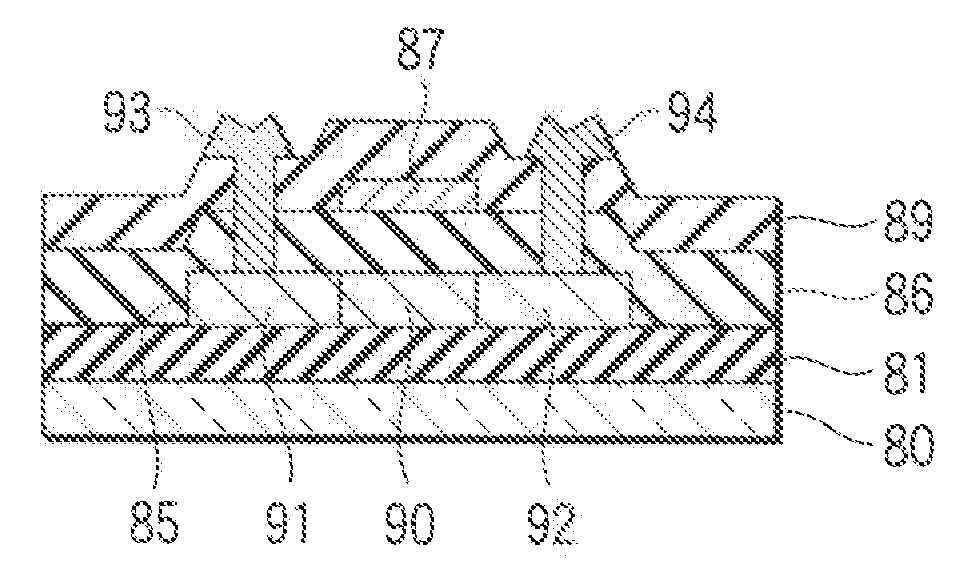
[0030]Hereinafter, a size of each crystal grain necessary for realizing a pair transistor structure and a basic concept of the present invention will be described, prior to the detailed description of an embodiment of the present invention. For example, in a crystal liquid display, a display panel is practically used in which an amorphous silicon film is formed on a glass substrate as an insulator, and a thin film transistor circuit is then formed by this amorphous silicon film. With digitization in an electron industry field, a high speed operation has been demanded, and the thin film transistor circuit of the high speed operation formed on a polycrystal silicon thin film has been put to practical use.

[0031]However, the polycrystal silicon thin film is constituted of polycrystal grains, and hence a plurality of grain boundaries or boundary lines are present in a channel region of each of the formed thin film transistors. The number of the boundary lines present in the channel regio...


PUM


Abstract

A crystal silicon array includes a crystallized unit region obtained by crystallizing at least a part of a non-single crystal semiconductor film. The crystallized unit region includes at least one square two-dimensional crystal portion having a size of 7 μm square or more, and at least one needle crystal portion having a grain length of 3.5 μm or more.

Description

CROSS-REFERENCE TO RELATED APPLICATIONS[0001]This application is based upon and claims the benefit of priority from prior Japanese Patent Application No. 2007-305325, filed Nov. 27, 2007, the entire contents of which are incorporated herein by reference.BACKGROUND OF THE INVENTION[0002]1. Field of the Invention[0003]The present invention relates to a crystal silicon array, and a manufacturing method of a thin film transistor. More particularly, it relates to a manufacturing method of a thin film transistor for use in a liquid crystal display, an organic EL display or the like, and a crystal silicon array suitable for the formation of the thin film transistor.[0004]2. Description of the Related Art[0005]A driving circuit of a display such as a liquid crystal display is usually formed by an amorphous semiconductor film formed on a glass substrate. With the enlargement of an IT market, information to be handled is digitized, and the processing of the information is speeded up. Hence, t...

Claims


Application Information

Patent Timeline
IPC IPC(8): H01L29/786H01L21/336
CPCH01L21/02381H01L21/02686H01L29/04H01L27/1296H01L27/1285
Inventor AZUMA, KAZUFUMISHIMOTO, SHIGEYUKIMATSUMURA, MASAKIYOENDO, TAKAHIKOTANIGUCHI, YUKIOKATO, TOMOYA
Owner ADVANCED LCD TECH DEVMENT CENT
Why Eureka
Try Eureka