Semiconductor device and method for controlling semiconductor device

a semiconductor device and semiconductor technology, applied in semiconductor devices, electronic switching, pulse techniques, etc., can solve the problems of difficult constant operation of sram in a stable manner and difficult control, and achieve high-speed operation of logic circuits and stable operation of memory circuits.

Active Publication Date: 2009-05-28
RENESAS ELECTRONICS CORP
View PDF8 Cites 218 Cited by
  • Summary
  • Abstract
  • Description
  • Claims
  • Application Information

AI Technical Summary

Benefits of technology

[0008]A main object of the present invention is to provide a semiconductor device having a thin-film BOX-SOI structure and provided with a logic circuit and a memory circuit on one semiconductor substrate, wherein a high-speed operation of a logic circuit and a stable operation of a memory circuit can be both achieved, and a method for controlling the semiconductor device.

Problems solved by technology

In a case where a conventional bulk transistor is used as the transistor in and after the 65-nm generation, it is difficult to control the threshold voltage variability to at most 40 mV, which, therefore, makes it difficult to constantly operate the SRAM in a stable manner.

Method used


Image

  • Semiconductor device and method for controlling semiconductor device
  • Semiconductor device and method for controlling semiconductor device
  • Semiconductor device and method for controlling semiconductor device

Examples


first embodiment

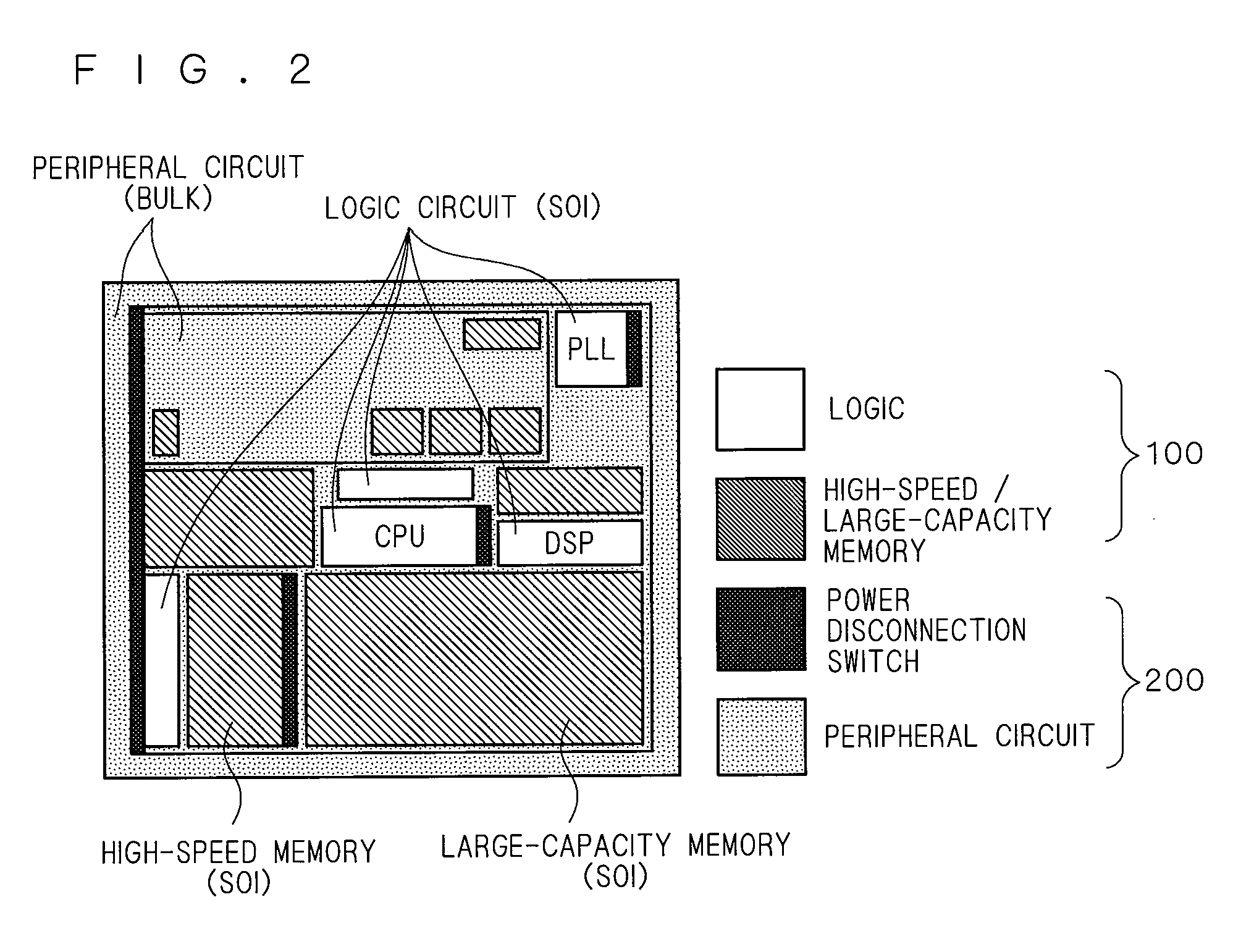
[0033]FIG. 2 illustrates an example of a floor plan of a semiconductor device. A SOI-MISFET (Metal Insulation Semiconductor Field Effect Transistor) 100 is used for the production of a logic circuit for which a high element performance is demanded and a high-speed memory circuit provided with a large capacity. A bulk MISFET 200 is used for the production of a power disconnection switch and peripheral circuits which requires a high pressure-resistant element. As a result, a system LSI (Large Scale Integration) capable of exerting a high performance, which is illustrated in FIG. 2, can be produced.

[0034]FIG. 3 illustrates an example where MEMS (Micro Electro Mechanical Systems) is also mixedly provided. The SOI-MISFET constitutes the LSI which requires a high-speed processing, and the MEMS such as a RF (Radio Frequency) module and a sensor are formed in a bulk region. As a result, a high-performance integrated circuit provided with the MEMS can be inexpensively provided.

[0035]FIG. 4 i...

second embodiment

[0112]A semiconductor device according to the present embodiment is configured such that the source / drain region is formed at a limited position relative to the gate electrode in the semiconductor device according to First Embodiment. The constitution other than the positional relationship between the gate electrode and the source / drain region, is the same as that of First Embodiment. Therefore, in the description below, the description of the same constitution is omitted, and only the different constitution (positional relationship between the gate electrode and the source / drain region) is described.

[0113]FIG. 26 is a schematic sectional view illustrating a positional relationship between the first gate electrode 20 and the source / drain regions8 and 9 constituting the first field-effect transistor described in First Embodiment. FIG. 26 is a schematic sectional view illustrating a positional relationship between a second gate electrode 20 and the source / drain regions 10 and 11 const...


PUM


Abstract

To provide a semiconductor device having a thin-film BOX-SOI structure and capable of realizing a high-speed operation of a logic circuit and a stable operation of a memory circuit. A semiconductor device according to the present invention includes a semiconductor support substrate, an insulation layer having a thickness of at mast 10 nm, and a semiconductor layer. In an upper surface of the semiconductor layer, a first field-effect transistor including a first gate electrode and constituting a logic circuit is formed. Further, in the upper surface of the semiconductor layer, a second field-effect transistor including a second gate electrode and constituting a memory circuit is formed. At least three well regions having different conductivity types are formed in the semiconductor support substrate. In the presence of the well regions, a region of the semiconductor support substrate below the first gate electrode and a region of the semiconductor support substrate below the second gate electrode are electrically separated from each other.

Description

BACKGROUND OF THE INVENTION[0001]1. Field of the Invention[0002]The present invention relates to a semiconductor device and a method for controlling the semiconductor device, and more particularly to a semiconductor device having the SOI structure and a method for controlling the semiconductor device.[0003]2. Description of the Background Art[0004]A SOI (Silicon On Insulating) device has a number of superior characteristics such as low power consumption, high-speed operation, and latch-up free. A thin-film BOX-SOI device, in which a BOX (Buried Oxide) layer is reduced in thickness to approximately 10 nm, in particular, has a planar double-gate structure. Therefore, the device is advantageous in that a short channel can be realized while a dopant concentration of the SOI layer is retained at a low level, and variability of a threshold voltage resulting from dopant-induced fluctuation, which has been increasingly evident in and after the 65-nm generation, can be lessened. For example,...

Claims


Application Information

Patent Timeline
Patent Type & Authority Applications(United States)
IPC IPC(8): H01L27/088
CPCH01L21/823878H01L21/84H01L27/105H01L27/1203H01L27/1104H01L27/1116H01L27/11H03K17/6872H10B10/18H10B10/00H10B10/12H01L29/0649
Inventor TSUCHIYA, RYUTAIWAMATSU, TOSHIAKI
Owner RENESAS ELECTRONICS CORP
Why Eureka
Try Eureka