

Semiconductor storage device
- Summary
- Abstract
- Description
- Claims
- Application Information
AI Technical Summary
Benefits of technology
Problems solved by technology
Method used
Image

Examples
embodiment 1
[0080](DRAM circuit)
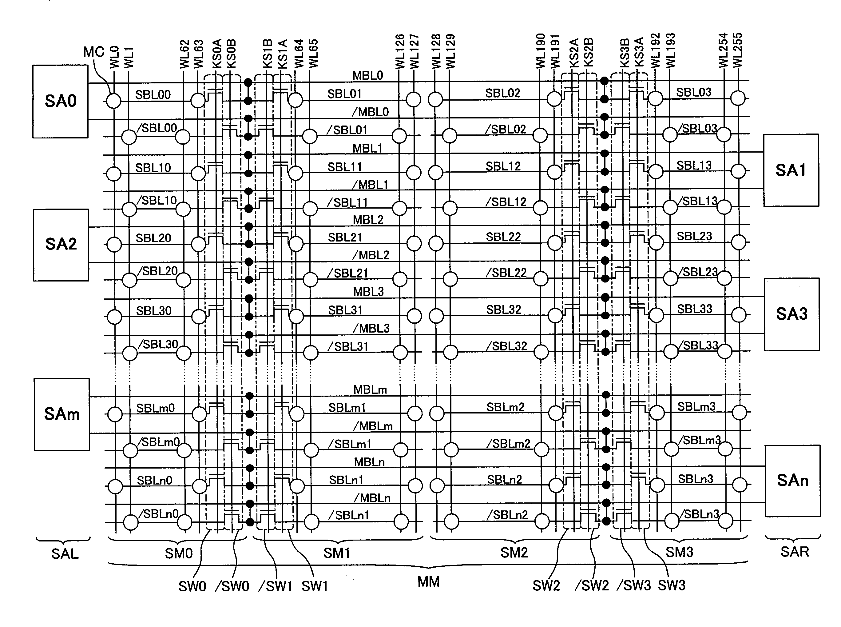
[0081]First, a DRAM circuit according to a first embodiment will be described with reference to FIG. 1.
[0082]This DRAM includes four sub memory arrays SM0 through SM3 in a main memory array MM and is configured to store data of 4×n bits×64 words. Bit lines for inputting / outputting stored data have a hierarchical bit-line architecture including main bit lines MBL0 through MBLn (and / MBL0 through / MBLn) and sub bit lines SBL00 through SBLn0, . . . SBL03 through SBLn3 (and / SBL00 through / SBLn0, . . . / SBL03 through / SBLn3). Each of the main bit lines is shared by the four sub memory arrays SM0 through SM3. The sub bit lines SBL00 through SBLn0, . . . SBL03 through SBLn3 (and / SBL00 through / SBLn0, . . . / SBL03 through / SBLn3) are respectively associated with the sub memory arrays SM0 through SM3. The bit lines also have a folded bit-line architecture.
[0083]Hereinafter, a portion of the sub memory array SM0 in which data of the first and second bits is stored will b...
PUM
 Abstract
Description
Claims
Application Information