Chemical mechanical polishing apparatus and method of chemical mechanical polishing
Inactive Publication Date: 2005-10-04
RENESAS ELECTRONICS CORP
View PDF13 Cites 1 Cited by
Summary
Abstract
Description
Claims
Application Information
AI Technical Summary
This helps you quickly interpret patents by identifying the three key elements:
Problems solved by technology
Method used
Benefits of technology
Benefits of technology
[0028]It is an object of the present invention to provide an apparatus for polishing a wafer, which apparatus is capable of enhancing uniformity in polishing. It is also an object of the present invention to provide a method of doing the same.
[0029]The inventors had conducted a lot of experiments in order to accomplish the above-mentioned object, and had found out that if a polishing pad is designed to include a region where there are formed no through-holes through which polishing slurry is supplied to a surface of the polishing pad, it would be possible to enhance uniformity in polishing a wafer.
[0047]In the apparatus in accordance with the present invention, a polishing pad is designed to have a region in which through-holes through which polishing material is supplied to a surface of the polishing pad are not formed. In the method in accordance with the present invention, polishing material is supplied to a surface of a polishing pad in a region other than a certain region of the polishing pad. As a result, the present invention makes it possible to accomplish uniformity in polishing rate in a high degree. Hence, when a buried metal layer is to be formed by chemical mechanical polishing, a resultantsemiconductor device could have superior resistance to electro-migration (EM).
Problems solved by technology
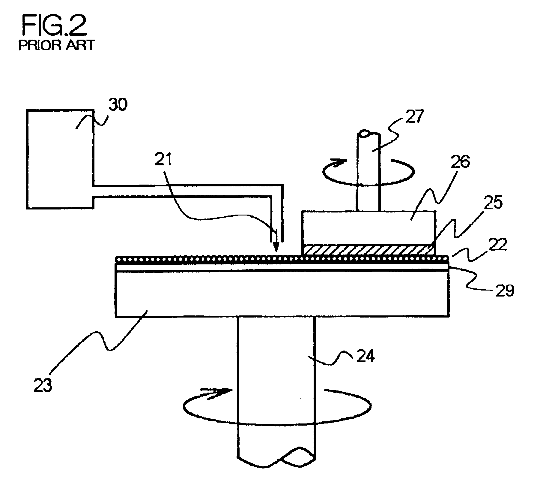
A conventional apparatus for polishing a wafer, such as the apparatus illustrated in FIG. 2, is accompanied with a problem of non-uniformity in polishing speed in a wafer, which results in that a wafer is polished around a center thereof to a greater degree than a periphery thereof.
Such a wafer having a great diameter could not be polished by means of such an apparatus as illustrated in FIG. 2, because the level block 23 has to have too much area, which results in too high load to the apparatus.
However, this may result in that a wiring to be formed on an insulating film has different heights above a central region and a peripheral region of a wafer.
Method used
Image
Click on the blue label to locate the original text in one second.
Reading with bidirectional positioning of images and text.
Examples
example 1
[0071]As a wafer to be polished, there was used a wafer which had a diameter of 8 inches (about 20 cm) and on which metal films composed of Cu, Ta, and TiN were formed. The wafer was polished by means of the apparatus illustrated in FIG. 3A. A polishing pad was formed uniformly with the through-holes, and had a diameter of 10 inches (about 25 cm).
[0072]The wafer was polished with the through-holes located closer to a center of the polishing pad, being closed one by one.
[0073]FIG. 5 shows uniformity in a polishing rate in this experiment. The uniformity was estimated with 3 σ (%). The polishing conditions were as follows.[0074]Pressure: 3 psi[0075]r.p.m.: 260 / 16[0076]Polishingslurry supply: 100 cc / minute
The polishing slurry having been employed in this experiment was commercially available one.
[0077]As is obvious in view of FIG. 5, the uniformity represented by 3σ is equal to or smaller than 15%, if the polishing pad had a circular region in which no through-holes are formed and whi...
example 2
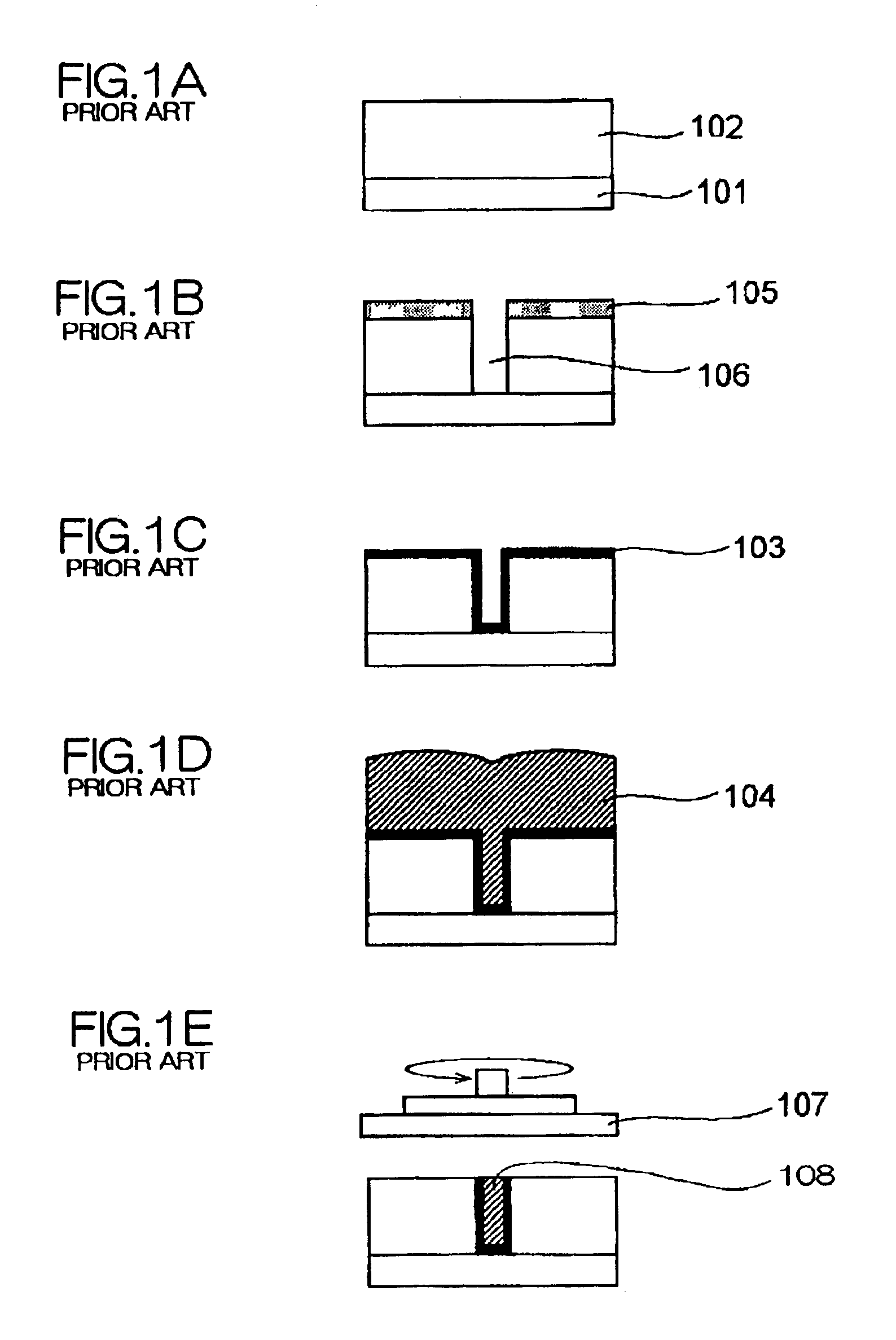
[0085]A semiconductor device was fabricated in accordance with the steps illustrated in FIGS. 1A to 1E.
[0086]First, as illustrated in FIG. 1A, a semiconductor substrate 101 including active devices fabricated thereon is covered entirely with an insulating film 102.
[0087]Then, a resist film 105 having a certain pattern is formed on the insulating film 102, and subsequently, the insulating film 102 is etched with the patterned resist film 105 being used as a mask, to thereby form a contact hole 106 through the insulating film 102, as illustrated in FIG. 1B.
[0088]After removal of the resist film 105, as illustrated in FIG. 1C, a barrier film 103 composed of metal such as Ti or Ta is deposited over the insulating film 102 so that the contact hole 106 is covered at a sidewall and a bottom thereof with the barrier film 103.
[0089]Then, as illustrated in FIG. 1D, an electrically conductive layer 104 composed of copper is deposited over the barrier film 103 to thereby fill the contact hole 1...
PUM
Property
Measurement
Unit
Fraction
aaaaa
aaaaa
Fraction
aaaaa
aaaaa
Fraction
aaaaa
aaaaa
Abstract
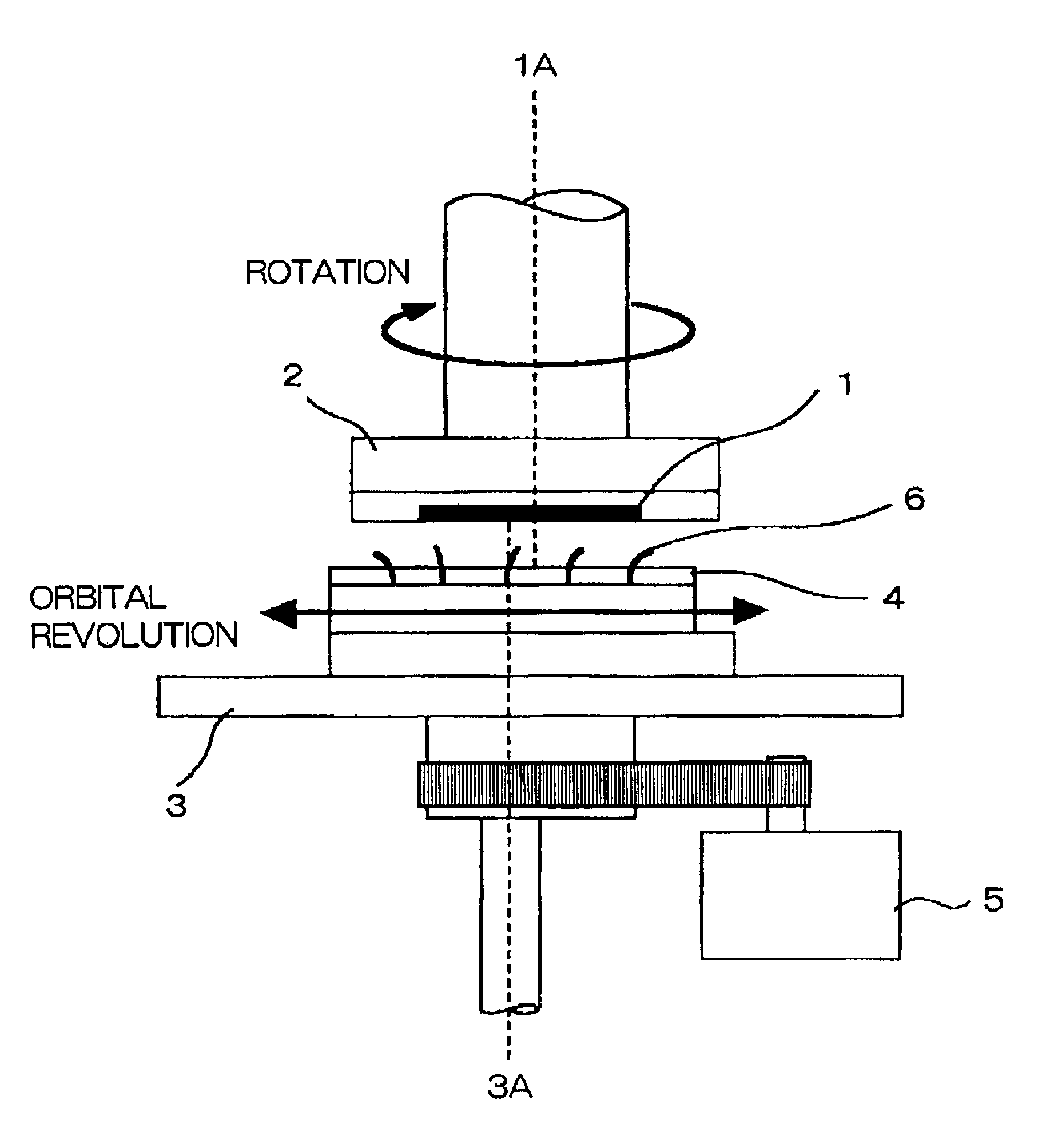
There is provided an apparatus for polishing a substrate, including (a) a polishing pad formed with a plurality of through-holes through which polishing material is supplied to a surface of the polishing pad, (b) a level block on which the polishing pad is mounted, and (c) a rotatable carrier for supporting a substrate thereon, the carrier being positioned in facing relation with the level block, the level block being rotatable around a rotation axis thereof with the rotation axis being moved along an arcuate path, and causing the polishing pad to make contact with the substrate for polishing the substrate, the polishing pad having a first ring-shaped region concentric thereto where no through-holes are formed. For instance, the first ring-shaped region has a width greater than 10%, but smaller than 95% of a radius of the polishing pad. The apparatus enhances uniformity in polishing a substrate.
Description
CROSS-REFERENCE TO RELATED APPLICATION[0001]This application is a Divisional of U.S. application Ser. No. 09 / 256,707, filed Feb. 24, 1999 now U.S. Pat. No. 6,783,446 issued Aug. 31, 2004.BACKGROUND OF THE INVENTION[0002]1. Field of the Invention[0003]The invention relates to an apparatus for polishing a substrate for planarization by chemical mechanical polishing. The invention relates further to a method of chemical mechanical polishing.[0004]2. Description of the Related Art[0005]FIGS. 1A to 1E illustrate respective steps in a method of forming a buried metal layer in a semiconductor device.[0006]First, as illustrated in FIG. 1A, a semiconductor substrate 101 including active devices fabricated thereon is covered entirely with an insulating film 102.[0007]Then, a resist film 105 having a certain pattern is formed on the insulating film 102, and subsequently, the insulating film 102 is etched with the patterned resist film 105 being used as a mask, to thereby form a contact hole 10...
Claims
Application Information
Patent Timeline
Application Date:The date an application was filed.
Publication Date:The date a patent or application was officially published.
First Publication Date:The earliest publication date of a patent with the same application number.
Issue Date:Publication date of the patent grant document.
PCT Entry Date:The Entry date of PCT National Phase.
Estimated Expiry Date:The statutory expiry date of a patent right according to the Patent Law, and it is the longest term of protection that the patent right can achieve without the termination of the patent right due to other reasons(Term extension factor has been taken into account ).
Invalid Date:Actual expiry date is based on effective date or publication date of legal transaction data of invalid patent.

