Optical Device Comprising a Waveguide Structure

a waveguide and optical device technology, applied in the direction of nanotechnology, instruments, nanotechnology, etc., can solve the problems of insufficient use of the waveguide and insignificant optical performance of the device, and achieve the effect of high free charge carrier density

Inactive Publication Date: 2009-05-28
BERINI PIERRE SIMON JOSEPH +2
View PDF0 Cites 15 Cited by
  • Summary
  • Abstract
  • Description
  • Claims
  • Application Information

AI Technical Summary

Benefits of technology

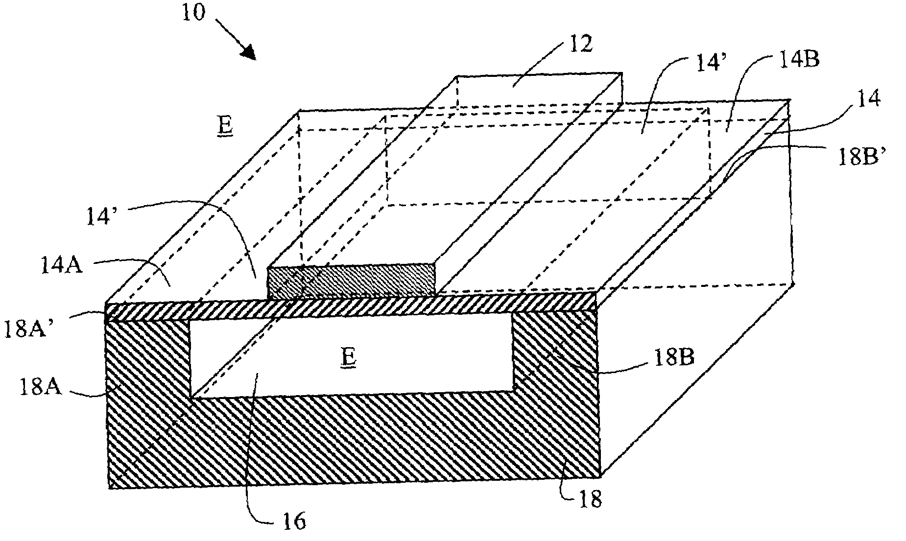
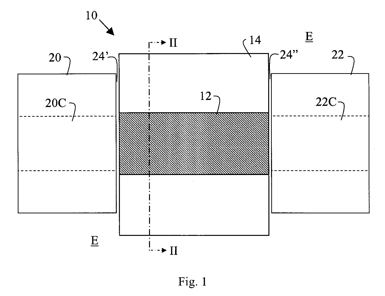
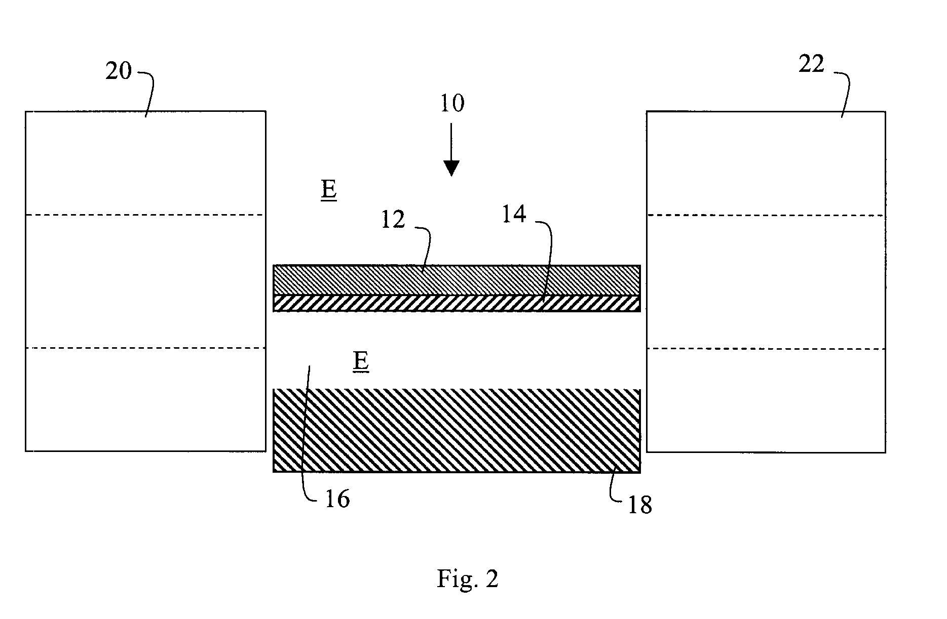
[0018]a thin strip having finite width and thickness of material having a relatively high free charge carrier density supported by a membrane having a predetermined thickness of material that has a relatively low free charge carrier density,
[0019]the dimensions of the width and thickness of the strip and the thickness of the supporting membrane bein...

Problems solved by technology

Following this convention, dimensions in general that are said to be “optically infinite” or “optically semi-infinite” are so large that they are insignificant t...

Method used


Image

  • Optical Device Comprising a Waveguide Structure
  • Optical Device Comprising a Waveguide Structure
  • Optical Device Comprising a Waveguide Structure

Examples


example 1

[0108]The free-space operating wavelength was set to 1550 nm, SiO2 (εr,2=1.4442) was selected as the material of the membrane 14, Au (εr,3=−131.95−j12.65) was selected as the material of the strip 12, and vacuum (εr,1=1) was selected as the environment E. The width w of the strip 12 was set to 8 μm, its thickness t was set to 30 nm, and the thickness d of the membrane 14 was varied from substantially 0 to about 65 nm for the purpose of illustrating its impact on the performance of the waveguide.

[0109]FIG. 6 gives the computed effective refractive index β / β0 of the ssb0 mode over the range of membrane thicknesses d. The effective refractive index of the TE0 and TM0 modes supported by the membrane 14 alone (i.e.: without the strip 12) was also plotted for reference.

[0110]FIG. 7 gives the computed attenuation of the ssb0 mode over the range of membrane thickness d, showing that the attenuation increases slightly with membrane thickness—indicating increasing confinement to the strip 12....

example 2

[0113]The free-space operating wavelength was set to 1310 nm, SiO2 (εr,2=1.44682) was selected as the material for the membrane 14, Au (εr,3=−86.08−j8.322) was selected as the material for the strip 12, and vacuum (εr,1=1) was selected for the environment E. The width w of the strip was set to 6 μm, its thickness t was set to 30 nm, and the thickness d of the membrane was varied from substantially 0 to about 55 nm for the purpose of illustrating its impact on the performance of the waveguide.

[0114]FIG. 9 gives the computed effective refractive index of the ssb0 mode over the range of membrane thickness. The effective index of the TE0 and TM0 modes supported by the membrane 14 alone (i.e.: without the strip 12) was also plotted for reference.

[0115]FIG. 10 gives the computed attenuation of the ssb0 mode over the range of membrane thicknesses d, showing that the attenuation increases slightly with membrane thickness—indicating increasing confinement to the strip 12. The attenuation rem...

example 3

[0118]The free-space operating wavelength was set to 1310 nm, SiO2 (εr,2=1.44682) was selected as the material of the membrane 14, Au (εr,3=−86.08−j8.322) was selected as the material of the strip 12, and water (εr,1=(1.3159−j1.639×10−5)2) was selected as the environment E. The width w of the strip 12 was set to 3 μm, its thickness / was set to 20 nm, and the thickness d of the membrane 14 was varied from substantially 0 to 100 nm for the purpose of illustrating its impact on the performance of the waveguide.

[0119]FIG. 12 gives the computed effective refractive index of the ssb0 mode over the range of membrane thicknesses. The effective index of the TE0 and TM0 modes supported by the membrane 14 alone (i.e.: without the strip 12) was also plotted for reference.

[0120]FIG. 13 gives the computed attenuation of the ssb0 mode over the range of membrane thickness, showing that the attenuation increases slightly with membrane thickness—indicating increasing confinement to the strip 12. The a...


PUM


Abstract

An optical device has a waveguide structure comprising a thin strip (12) having finite width and thickness of material having a relatively high free charge carrier density supported by a membrane (14) having a predetermined thickness of material that has a relatively low free charge carrier density. The dimensions of the width and thickness of the strip and the thickness of the supporting membrane are such that, when the waveguide structure is surrounded at least partially by an environment (E) having a low free charge carrier density, optical radiation having a wavelength in a predetermined range couples to the waveguide structure and propagates along the length thereof as a plasmon-polariton wave that permeates at least part of the environment (E).

Description

CROSS-REFERENCE TO RELATED APPLICATION[0001]This application claims priority from U.S. Provisional patent applications Nos. 60 / 694,667 filed Jun. 29, 2005 and 60 / 794,825 filed Apr. 26, 2006, the contents of which are incorporated herein by reference.TECHNICAL FIELD[0002]The invention relates to optical devices comprising a waveguide structure, particularly for guiding surface plasmon-polariton waves, and is especially, but not exclusively, applicable to optical devices for use in sensing constituents of or bodies in fluids.BACKGROUND[0003]In the context of this patent specification:[0004]The term “optical radiation” embraces electromagnetic waves having wavelengths in the infrared, visible and ultraviolet ranges.[0005]The terms “finite” and “infinite” as used herein are used by persons skilled in this art to distinguish between waveguides having “finite” widths in which the actual width is significant to the performance of the waveguide and the physics governing its operation and so...

Claims


Application Information

Patent Timeline
IPC IPC(8): G02B6/10G02B6/24
CPCB82Y20/00G01N21/553G02B6/1226G02B2006/12159G02B2006/12147G02B2006/1215G02B6/30
Inventor BERINI, PIERRE SIMON JOSEPHCHARBONNEAU, ROBERTLAHOUD, NANCY
Owner BERINI PIERRE SIMON JOSEPH
Why Eureka
Try Eureka