

Boundary scan method, system and device
- Summary
- Abstract
- Description
- Claims
- Application Information
AI Technical Summary
Benefits of technology
Problems solved by technology
Method used
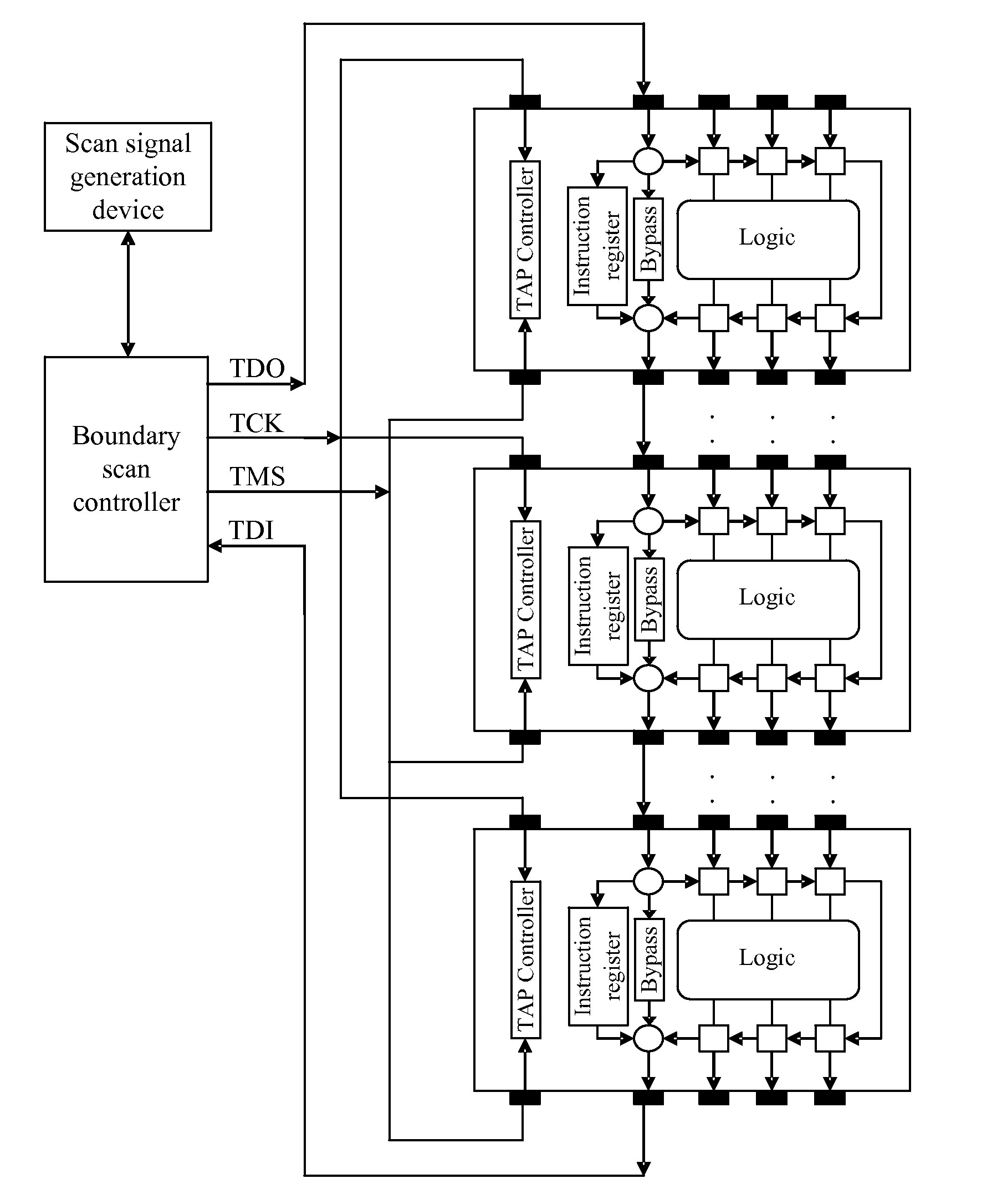
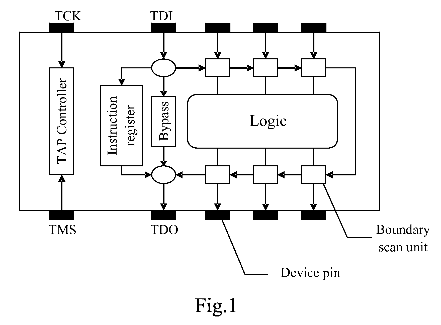
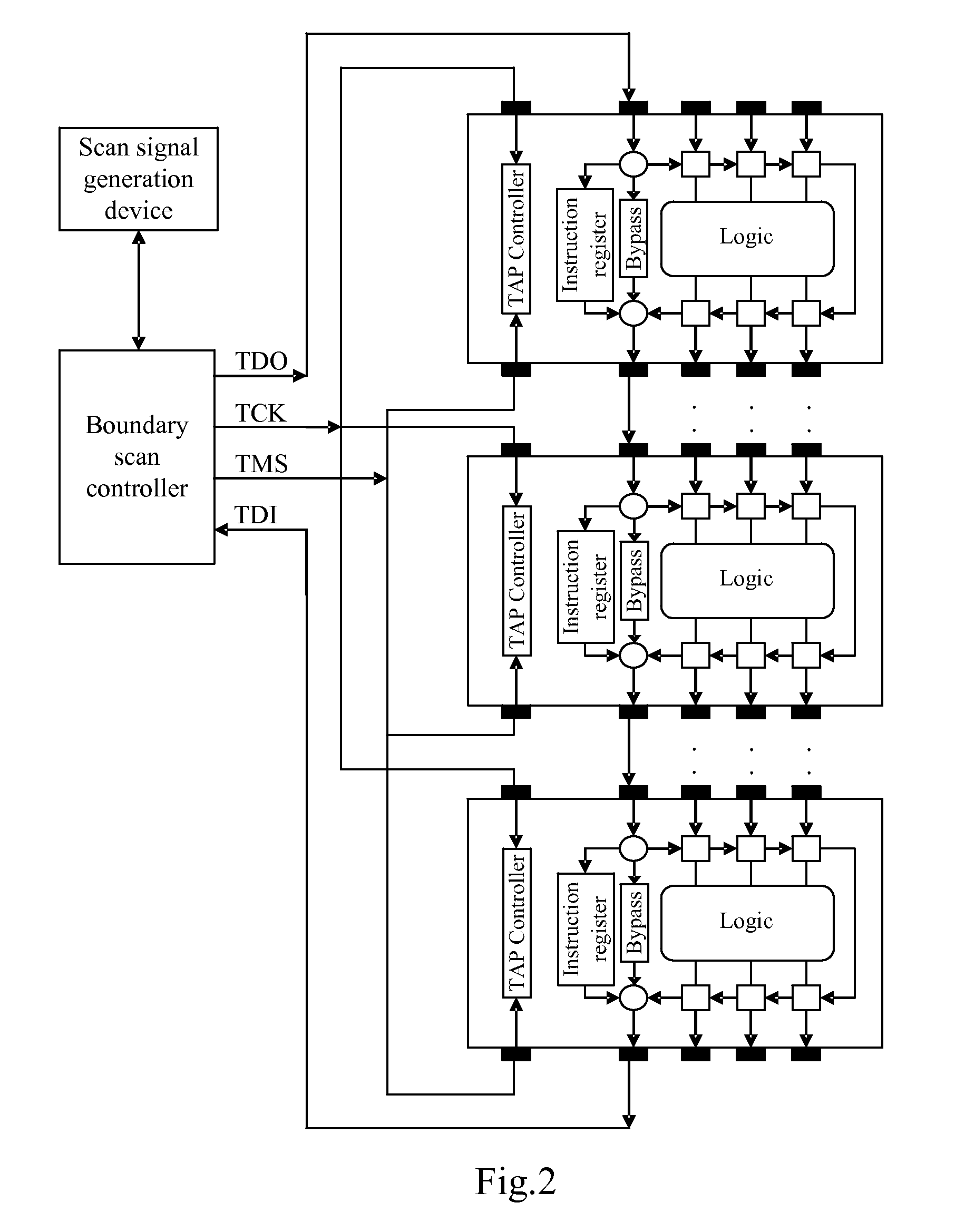
Image

Examples
Embodiment Construction
[0023]A general implementation principle, specific implementations and advantageous effects that can be attained correspondingly of the embodiments of the invention will be set forth in details hereinafter with reference to the respective figures in the drawings.
[0024]Referring to FIG. 3, it illustrates a flow chart of a boundary scan method according to an embodiment of the invention, which generally includes the following steps:
[0025]In step S10, a scan signal generation apparatus generates first parallel unipolarity boundary scan signals, and sends them to a boundary scan controller.
[0026]In step S11, the boundary scan controller performs parallel-to-serial conversion of the first parallel unipolarity boundary scan signals output from the scan signal generation apparatus and generates a clock signal and a status control signal in accordance with the received first parallel boundary scan signals.
[0027]In step S12, the boundary scan controller outputs serial differential unipolarit...
PUM
 Abstract
Description
Claims
Application Information