Imaging device

a technology of imaging device and temperature detection, which is applied in the field of imaging device, can solve the problems of increasing manufacturing cost, deteriorating accuracy of temperature detection, and inability to compact the entire imaging device, so as to reduce the manufacturing cost of the imaging device, and minimize the effect of the imaging devi

Inactive Publication Date: 2009-06-04
KONICA MINOLTA INC
View PDF5 Cites 25 Cited by
  • Summary
  • Abstract
  • Description
  • Claims
  • Application Information

AI Technical Summary

Benefits of technology

[0033]According to the invention described in claim 1, the manufacturing cost of the imaging device is reduced and the imaging device can be minimized as a whole, and the temperature of the imaging area can be detected accurately.
[0034]According to the invention described in claim 2, precise temperature compensation for the temperature characteristic of the imaging element is possible.
[0035]According to the invention described in claim 3, in the imaging device including a linear log sensor, temperature compensation for the temperature characteristic of the linear log sensor is possible. According to the invention described in claim 4, by providing the imaging element capable of switching between the plurality of linear conversion characteristics (different inclination), the fluctuation of incline of linear conversion character caused by change of the temperature and the fluctuation of the changeover point can be compensated.
[0036]According to the invention described in claim 5, by detecting the temperature of the imaging area accurately, more precise temperature compensation for the temperature characteristic of the imaging element is possible.
[0037]According to the invention described in claim 6, since the temperature of the most desirable area to be measured within the imaging area is detected by the temperature sensor, effective temperature compensation becomes possible.
[0038]According to the invention described in claim 7, since the temperature sensor is provided in the imaging area of the imaging element, accurate temperature detection can be realized without temperature detection being varied.

Problems solved by technology

However, in the imaging device described in the Patent document 1, since the imaging element and the temperature sensor are configured as different members, a physical distance between them becomes large, thus an accuracy of temperature detection is deteriorated and a manufacturing cost increases due to an additional assembling process of the temperature sensor.
Also, in the imaging device described in the Patent document 2, though the temperature sensor is provided in the vicinity of the imaging element, the imaging element, the temperature sensor and an electronic circuit are configured as different members, there was a problem that an entire imaging device cannot be compact.
Also, in a case where due to a layout and a shape a contact area with the imaging element cannot be large, the temperature of the imaging element was not able to detect accurately.
Also, in the imaging device described in the Patent document 3, though the temperature sensor is provided on the imaging element, since the temperature sensor is not located in the imaging area of the imaging element and located in the periphery of the imaging area, there was a problem that the temperature of the imaging area was not able to detect accurately.

Method used


Image

  • Imaging device
  • Imaging device
  • Imaging device

Examples


first embodiment

[0078]A first embodiment of the present invention will be described with reference to FIG. 1 to FIG. 8.

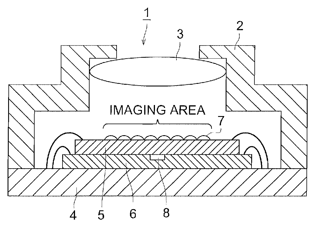
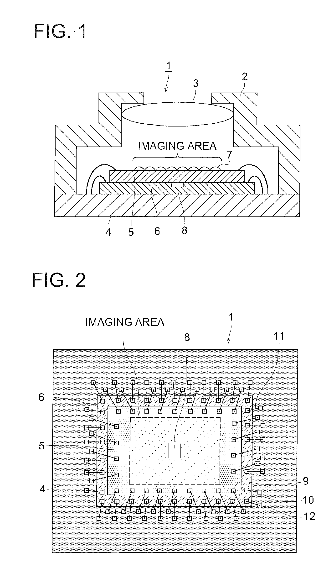
[0079]As FIG. 1 shows, an imaging device 1 is provided with a housing 2 and in a vicinity of a center section of one side surface of the housing 2, a lens 3 to condense image light of an object at a prescribed Focal point is provided in a way that a light axis of the lens 3 is orthogonal to a light receiving surface of the imaging element 5.

[0080]Also, a substrate 4 is provide inside the housing 2, on which a signal processing chip 6 and imaging element 5 are respectively stacked via thin adhesion layers (unillustrated). Meanwhile, for the adhesion layer, a resin having a high thermal conductivity is preferred to be used.

[0081]The imaging element 5 to perform photoelectric conversion where reflected light of the object coming through a lens 3 is converted into an electric signal is provided at a back surface of the lens 3. Also, a surface opposed to the lens 3 of the imaging elemen...

second embodiment

[0169]A second embodiment of the present invention will be described with reference to FIG. 9. Meanwhile, the same portions as that in the first embodiment are denoted by the same symbols and the description thereof is omitted, thus configurations and operations different from that in the first embodiment will be described.

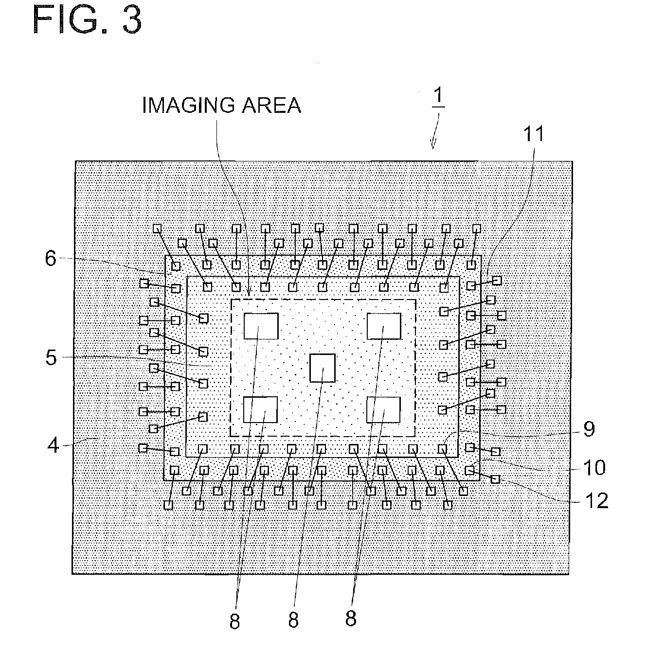
[0170]Aspects where the imaging device 1 is provided with a housing 2, a lens 3, a substrate 4, an imaging element 5 and a signal processing chip 6, and a temperature sensor 8 is integrated in the signal processing chip 6 are the same as that of the first embodiment.

[0171]Here, as FIG. 9 shows, at a vicinity of an edge of the imaging element 5 of the present embodiment, a plurality of holes 32 for wiring to lace wires connected with electrode pads 9 are formed. Also, at a vicinity of an edge of the signal processing chip 6, a plurality of holes 33 to lace wires connected to electrode pads 10 are formed.

[0172]Also, on a rear surface side of the imaging element 5, t...


PUM

PropertyMeasurementUnit
temperatureaaaaaaaaaa
areaaaaaaaaaaa
electricaaaaaaaaaa

Abstract

The present invention provides an imaging device where the temperature of an imaging area of the imaging device is accurately detected to perform precise temperature compensation and the imaging device can be minimized as a whole. This imaging device is characterized in that the device includes: the imaging element (5) for converting incident light into an electric signal; a signal processing chip (6) mounted by being stacked with the imaging element (5); and a temperature sensor (8) integrated into the signal processing chip (6) close to the imaging element (5) in a state where the imaging element (5) and the signal processing chip (6) are stacked.

Description

FIELD OF THE INVENTION[0001]The present invention relates to an imaging device having an imaging element particularly having a temperature characteristic.BACKGROUND[0002]An imaging element for photoelectric conversion to convert incidentlight to an electric signal has been provided for an imaging device such as a camera unit integrated in a digital camera or an onboard camera. As the imaging element, CCD (Charging Couple Device) type image sensor or CMOS (Complementary Metal-Oxide Semiconductor) type image sensor has been widely used.[0003]Since the CCD type image sensor and CMOS image sensor have a temperature characteristic, there has been known an imaging device that according to a temperature inside an imaging device detected by a sensor, a compensation amount of image data obtained by the image sensor is calculated and the photographed image is compensated so as to obtain an optimum image.[0004]For example, in a Patent Document 1, there is described an imaging device where vari...

Claims


Application Information

Patent Timeline
Patent Type & Authority Applications(United States)
IPC IPC(8): H01J40/14G01K13/00H04N5/355H04N5/361
CPCH01L27/14618H01L31/0232H04N5/361H04N5/2257H04N5/35518H04N5/2253H01L2224/05554H01L2224/48091H01L2224/49171H04N23/54H04N23/57H04N25/573H04N25/63H01L2924/00014
Inventor TAKAYAMA, JUN
Owner KONICA MINOLTA INC
Why Eureka
Try Eureka