Electron beam writing method, fine pattern writing system, method for manufacturing uneven pattern carrying substrate, and method for manufacturing magnetic disk medium

a writing system and writing method technology, applied in the field of electroctron bean writing method and a, can solve the problems of difficult to change intensity, difficult to accurately write elements, etc., and achieve the effect of high accuracy, easy manufacturing, and excellent properties

Inactive Publication Date: 2009-06-04
FUJIFILM CORP
View PDF2 Cites 8 Cited by
  • Summary
  • Abstract
  • Description
  • Claims
  • Application Information

AI Technical Summary

Benefits of technology

[0024]Further, the deflection speed of the electron beam in the direction orthogonal to the radius direction of the rotation stage may be controlled so as to be fast in writing on an inner circumferential track and slow in writing on an outer circumferential track in inversely proportional to the radius of the writing position on the substrate.
[0032]According to the electron beam writing method of the present invention, an electron beam is scanned by an electron beam writing unit capable of XY deflecting the electron beam in which the electron beam is shifted in a radius direction and a direction orthogonal to the radius direction of the rotation stage while a substrate applied with a resist and placed on a rotation stage is rotated in one direction to write a fine pattern, which is constituted by elements having a track direction length greater than a radiation diameter of the electron beam, on the substrate. Here, the electron beam is scan controlled so as to completely fill the shape of each of the elements by vibrating the electron beam rapidly in the radius direction of the rotation stage and at the same time deflecting in the direction orthogonal to the radius direction of the rotation stage faster than a rotational speed thereof, thereby the elements are written sequentially. This increases the flexibility to control the amount of radiation exposure in scan writing with an electron beam, whereby a fine pattern having a complicated shape which is to be formed on a magnetic disk medium may be written over the entire surface of the substrate highly accurately. That is, the writing may be performed with a constant amount of radiation exposure over the entire surface of the substrate rapidly and accurately, whereby writing efficiency is improved and the writing time is reduced.
[0033]In particular, the electron beam is deflected in the direction orthogonal to the radius direction of the rotation stage faster than a rotational speed thereof, so that writing in the forward direction with respect to the rotation is possible. This provides a time allowance to appropriately control the amount of radiation exposure according to the element shape of the fine pattern. For example, for an element that requires more amount of radiation exposure, the scanning speed of the electron beam may be decreased, while a groove pattern of a discrete track medium that tends to be overexposed may be written with an appropriate amount of radiation exposure by writing the pattern in a small width with a greater deflection speed in the direction opposite to the rotational direction of the rotation stage.
[0034]Further, the flexibility in arranging elements of a fine pattern is increased, whereby, for example, a first element is written in the forward direction, then the electron beam is returned in the backward direction, and a second element overlapping in phase with the first element may be written. As such, a wide variety of patterns may be written. Still further, a time required for synchronization and alignment between the rotation of the rotation stage and writing is ensured, so that the writing accuracy is further improved.
[0035]In the mean time, the fine pattern writing system for realizing the electron beam writing method of the present invention includes a signal output unit for outputting a write data signal and an electron beam writing unit for scanning an electron beam, so that a desired fine pattern may be written rapidly and highly accurately, whereby writing efficiency is improved and the writing time is reduced.
[0037]According to the method for manufacturing an uneven pattern carrying substrate of the present invention, the method includes the step of exposing a desired fine pattern on a substrate applied with a resist by the electron beam writing method described above and forming an uneven pattern thereon corresponding to the desired fine pattern. Thus, a substrate having thereon a highly accurate uneven pattern may be obtained easily. Where the substrate is an imprint mold, in particular, the use of the mold in patterning using an imprint technology allows a magnetic disk medium having excellent properties, such as a discrete track medium or a bit pattern medium, to be manufactured easily in which the mold is pressed onto the surface of a resin layer to be used as a mask in the manufacturing process of the magnetic disk medium and the pattern is transferred to the surface of the medium at a time. Where the substrate is a magnetic transfer master substrate, the substrate has thereon a fine pattern of a magnetic layer which includes at least a servo pattern, so that the use of the master substrate allows a magnetic recording medium having excellent properties to be manufactured easily in which the master is brought into contact with the magnetic recording medium and a magnetic field is applied thereto using a magnetic transfer technology and a magnetic pattern corresponding to the pattern of the magnetic layer is transfer formed on the magnetic recording medium.

Problems solved by technology

In the mean time, when writing fine patterns by the electron beam writing methods described above, it is difficult to accurately write elements which form each pattern over the entire tracks from the innermost circumferential track to the outermost circumferential track with a uniform amount (dose amount) of radiation exposure.
In particular, for those that vibrate the electron beam in the radius or circumferential directions, it is difficult write a pattern which includes elements having different lengths in the radius directions (track width directions) or circumferential directions (track directions) with a uniform amount of radiation exposure.
The reason is that the change in the beam intensity of the electron beam causes beam instability so that the beam intensity can not be changed during the writing of elements according to the shapes of the elements.
But, when writing the groove pattern for separating the adjacent track described above following the servo pattern, if the electron beam is fixedly irradiated to write the groove pattern in an arc shape by the rotation of the substrate, the electron beam intensity for the servo pattern writing is too intense for the groove writing since the groove pattern has a narrow width in the radius directions and continued in the track directions.
Consequently, the line width becomes larger by exposure bleeding, thereby posing a problem that writing of a groove pattern having a predetermined width relative to the track width can not be performed.
Such deflection control alone is insufficient for the flexibility in the change of radiation exposure amount and can not address the problem described above.
But, the method has a problem that it takes a lot of time to write a pattern over the entire substrate and it is difficult to perform pattern writing over the entire substrate by ensuring on / off positional accuracy of the electron beam according to the rotational position in inner and outer circumferences.

Method used


Image

  • Electron beam writing method, fine pattern writing system, method for manufacturing uneven pattern carrying substrate, and method for manufacturing magnetic disk medium
  • Electron beam writing method, fine pattern writing system, method for manufacturing uneven pattern carrying substrate, and method for manufacturing magnetic disk medium
  • Electron beam writing method, fine pattern writing system, method for manufacturing uneven pattern carrying substrate, and method for manufacturing magnetic disk medium

Examples


Embodiment Construction

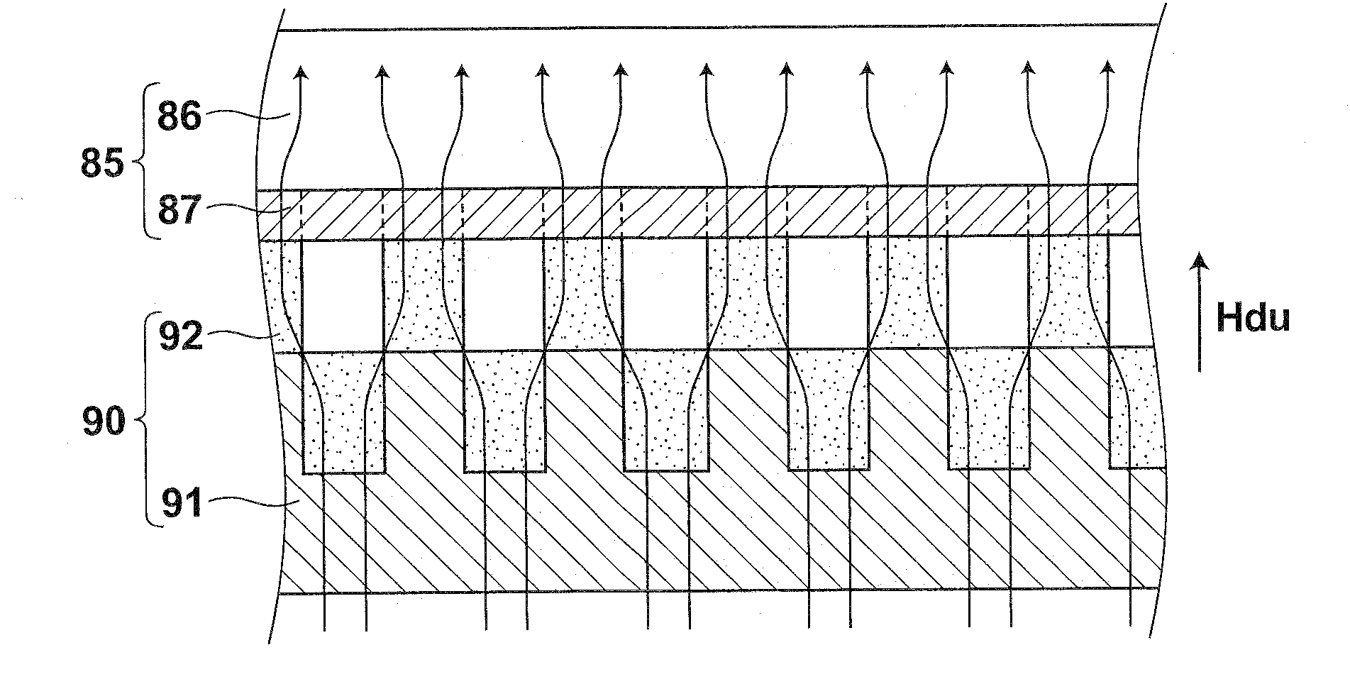
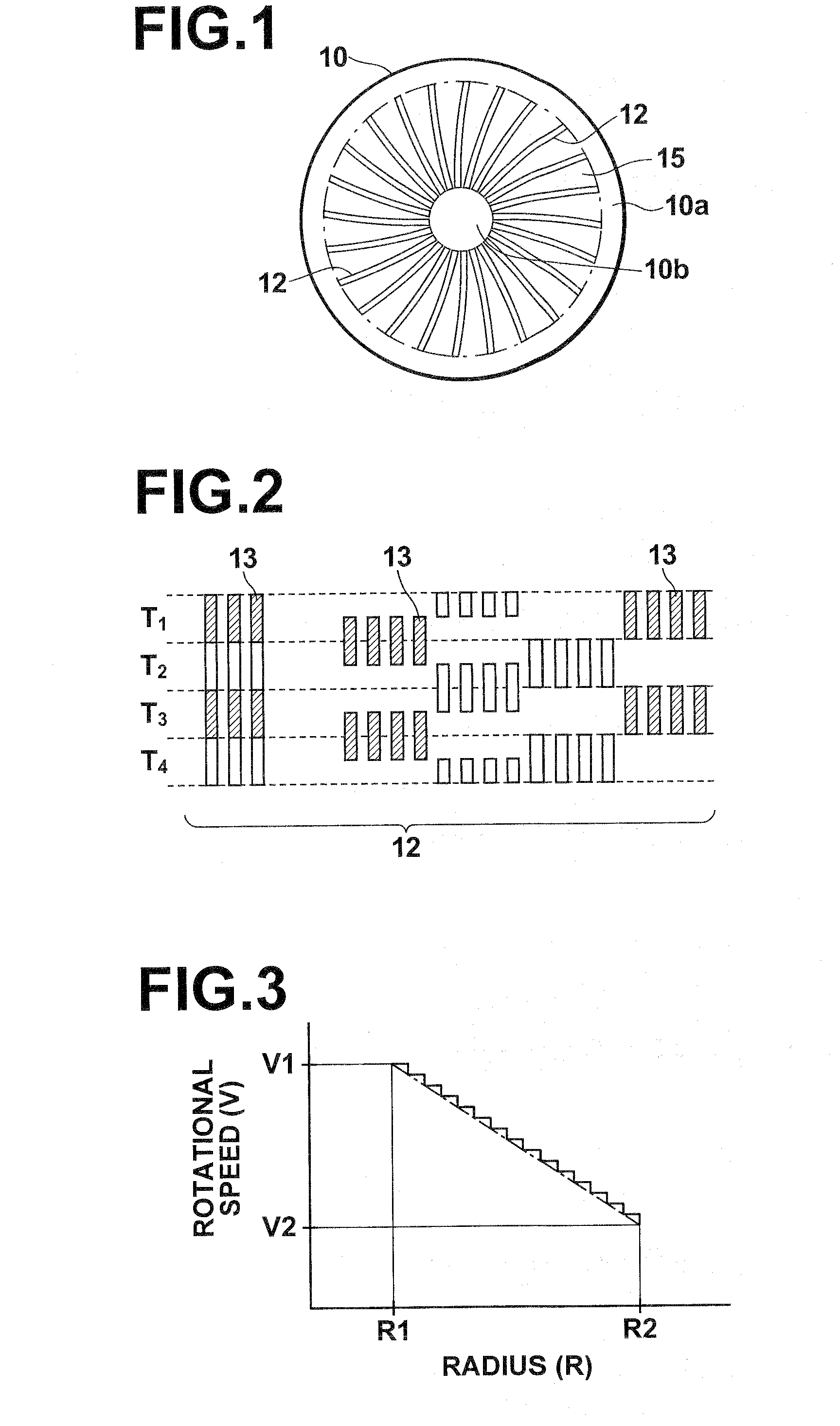
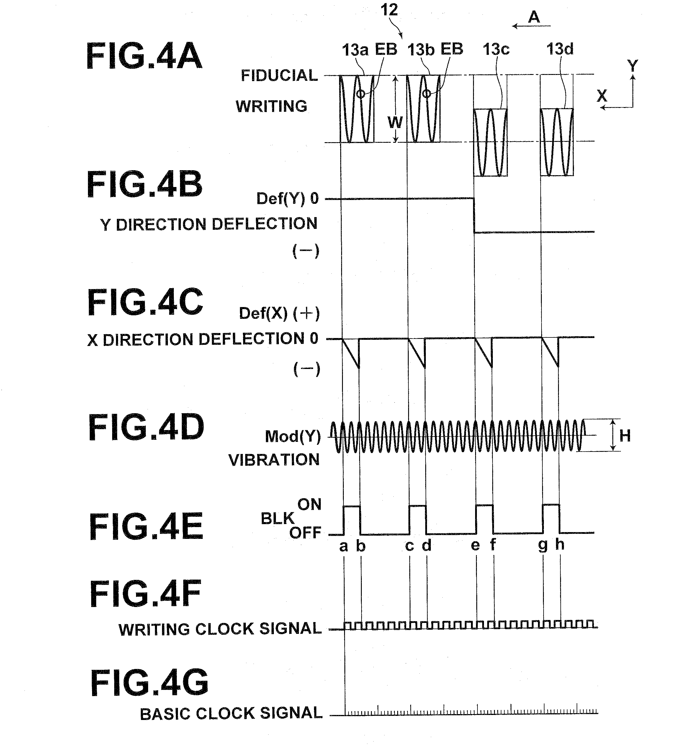
[0049]Hereinafter, exemplary embodiments of the present invention will be described in detail with reference to the accompanying drawings. FIG. 1 illustrates an example fine pattern in plan view to be written on a substrate by an electron beam writing method of the present invention. FIG. 2 is a partially enlarged view of the fine pattern. FIG. 3 is a graph illustrating the relationship between the writing radius position and substrate rotational speed. FIG. 4A is an enlarged schematic view of a basic writing principle for writing elements constituting a fine pattern on inner circumferential tracks, and FIGS. 4B to 4G illustrate various signals, including a deflection signal and the like, used in the basic writing principle shown in FIG. 4A. FIG. 5A is an enlarged schematic view of a basic writing principle for writing elements constituting an identical fine pattern to that shown in FIG. 4A on outer circumferential tracks, and FIGS. 5B to 5G illustrate various signals, including a d...


PUM

PropertyMeasurementUnit
radiation diameteraaaaaaaaaa
rotational angleaaaaaaaaaa
lengthaaaaaaaaaa

Abstract

When writing elements of a fine pattern on a substrate applied with a resist by scanning an electron beam on the substrate, the electron beam is scan controlled so as to completely fill the shape of each of the elements by vibrating the electron beam rapidly in a radius direction of the rotation stage and at the same time deflecting in a direction orthogonal to the radius direction of the rotation stage faster than a rotational speed thereof, thereby sequentially writing the elements.

Description

BACKGROUND OF THE INVENTION[0001]1. Field of the Invention The present invention relates to an electron bean writing method and a fine pattern writing system for writing a fine pattern according to a desired uneven pattern when manufacturing an imprint mold, magnetic transfer master substrate, or the like for a high density magnetic recording medium, such as a discrete track medium, bit pattern medium, or the like.[0002]The present invention also relates to a method for manufacturing an uneven pattern carrying substrate that includes an imprint mold, magnetic transfer master substrate, or the like having an uneven pattern surface formed through a writing step performed by the electron beam writing method described above. The invention further relates to a method for manufacturing a magnetic disk medium having an uneven pattern transferred thereto from the uneven pattern carrying substrate or imprint mold, and a method for manufacturing a magnetic disk medium having a magnetized patt...

Claims


Application Information

Patent Timeline
Patent Type & Authority Applications(United States)
IPC IPC(8): H01J3/14G03F7/20A61N5/00
CPCB82Y10/00H01J37/3174B82Y40/00Y10S430/143
Inventor KOMATSU, KAZUNORIUSA, TOSHIHIRO
Owner FUJIFILM CORP
Why Eureka
Try Eureka