Variable threshold trench IGBT with offset emitter contacts

a technology of offset emitter contacts and trench igbts, which is applied in the direction of transistors, electrical devices, semiconductor devices, etc., can solve the thermal limitation of the scsoa of today's igbts, achieve enhanced parasitic thyristor latch-up, reduce field crowding, and reduce the overall channel density of the device

Active Publication Date: 2009-06-11
INFINEON TECH AMERICAS CORP
View PDF13 Cites 13 Cited by
  • Summary
  • Abstract
  • Description
  • Claims
  • Application Information

AI Technical Summary

Benefits of technology

[0019]In order to achieve the desired channel density and breakdown voltage, narrow cell pitch is needed to reduce field crowding in which only a portion of the channels are conducting. One method for obtaining a desirable combination of channel density and breakdown voltage is shorting every other trench poly gate to emitter. Shorting gate to emitter eliminates gate drive completely for specific trenches, effectively reducing the overall channel density of the device while maintaining a narrow cell pitch to achieve the desired breakdown voltage. A structure using the latter method has been published in ISPSD 2006 by Mitsubishi, which has been defined as a damping trench for eliminating switching oscillations.
[0020]According to the present invention the saturation current of the IGBT is reduced in a unique manner to achieve the desired SCSOA. Specifically, according to the present invention,

Problems solved by technology

Since type D failure is thermally limited,

Method used


Image

  • Variable threshold trench IGBT with offset emitter contacts
  • Variable threshold trench IGBT with offset emitter contacts
  • Variable threshold trench IGBT with offset emitter contacts

Examples


Embodiment Construction

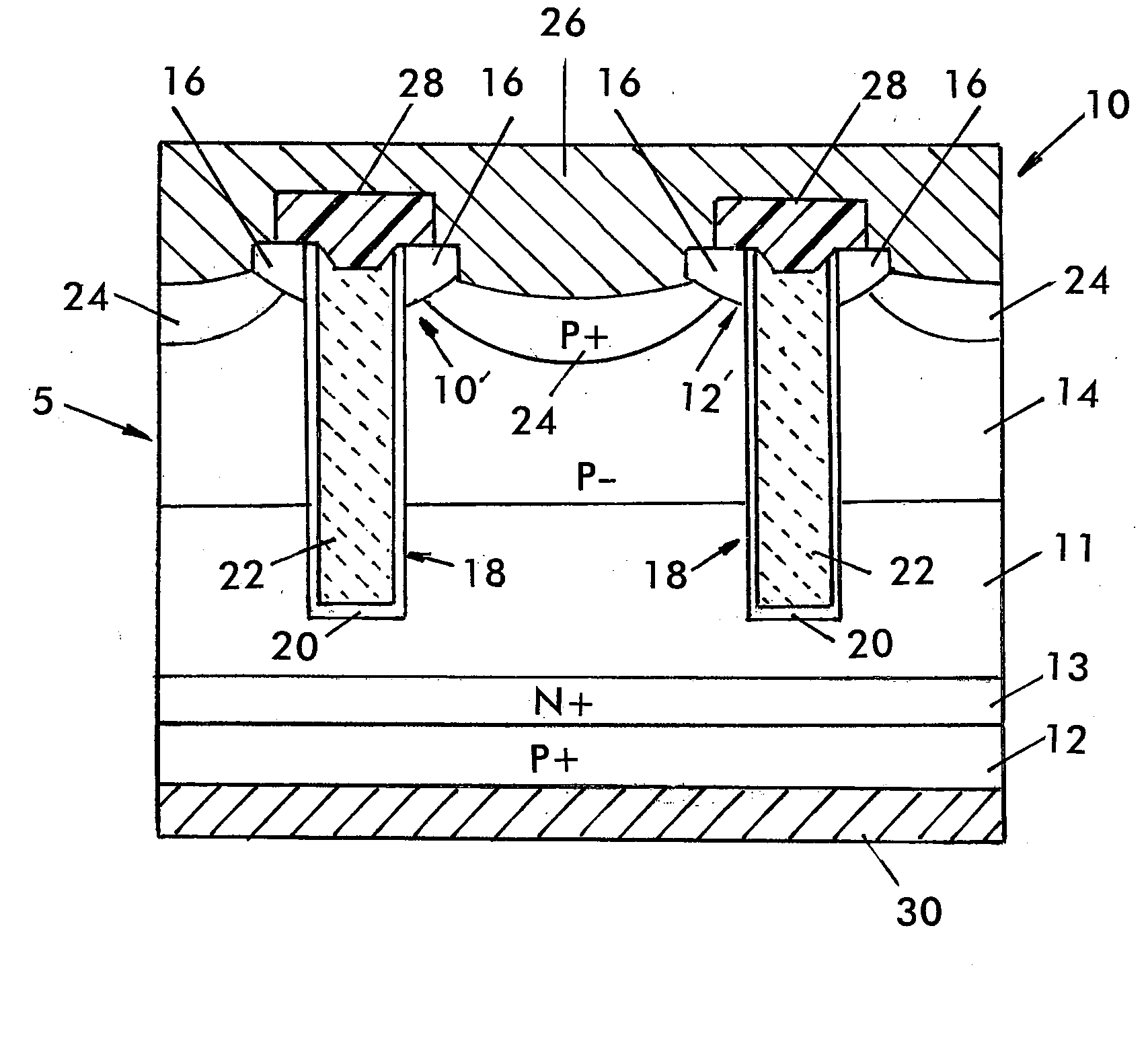
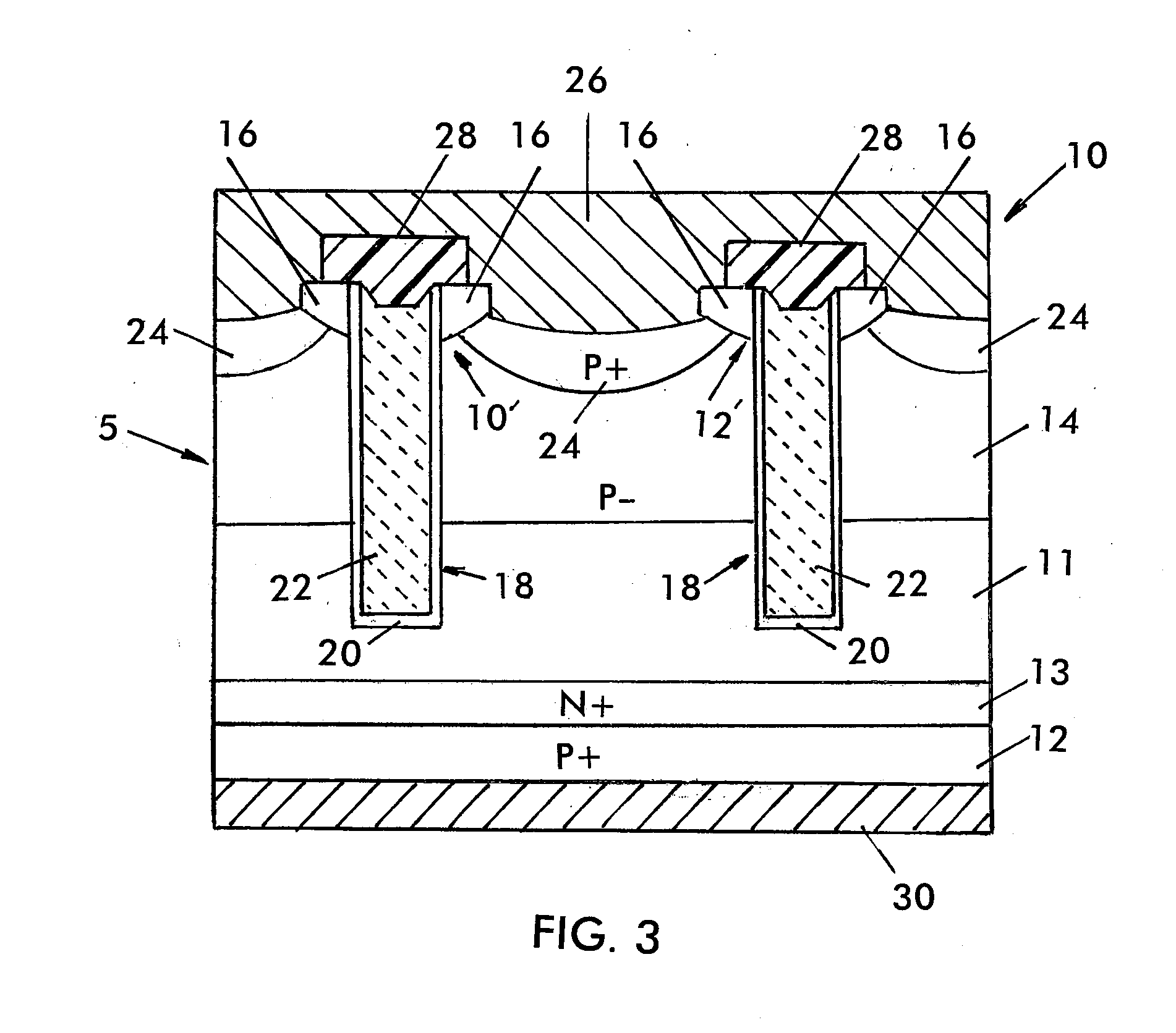
[0027]Referring to FIG. 3, a semiconductor device 10 according to the present invention is an IGBT that comprises semiconductive body 5 which includes first region 14 (base region) of a first conductivity type, e.g. P type, disposed over second region 11 (drift region) of a second conductivity type, e.g. N type, and diffused regions 16 (emitter regions) of the second conductivity type. Emitter regions 16 are formed in base region 14 adjacent to opposing walls of trenches 18, which extend from the top surface of semiconductive body 5 to a depth that is below the depth of base region 14. Each trench 18 is lined with a thin gate insulation layer 20, for example, a silicon dioxide layer, and filled with a conductive gate material 22, such as, conductive polysilicon, to form an insulated gate structure.

[0028]Semiconductor device 10 also includes high conductivity emitter contact regions 24 of the first conductivity type which extend to a predetermined depth into base region 14. Emitter c...


PUM


Abstract

A trench type IGBT as disclosed herein includes a plurality of channel regions having one threshold voltage for the normal operation of the device and a plurality of channel regions having a threshold voltage higher than the threshold voltage for the normal operation of the device.

Description

CROSS-REFERENCE TO RELATED APPLICATION[0001]The present application is based on and claims priority to U.S. Provisional Patent Application Ser. No. 60 / 999,240, filed on Oct. 17, 2007 and entitled VARIABLE THRESHOLD TRENCH IGBT WITH OFFSET EMITTER CONTACTS, the entire disclosure of which is hereby incorporated by reference.FIELD OF INVENTION[0002]The present invention relates to a technique for designing and fabricating a trench IGBT (insulated gate bipolar transistor) to increase device robustness in motor drive inverters among other applications and an IGBT fabricated according to the method.BACKGROUND AND SUMMARY OF THE INVENTION[0003]In industrial motor drive applications, an IGBT with a long short-circuit withstand time (SCSOA) is required. The withstand time represents how long the IGBT can stay functional and be turned off after encountering a motor fault condition where the IGBT conducts under full bus voltage (collector-emitter voltage). The withstand time is required for th...

Claims


Application Information

Patent Timeline
IPC IPC(8): H01L29/739
CPCH01L29/0839H01L29/7397H01L29/1095
Inventor NG, CHIUCHAO, YUAN-HENG
Owner INFINEON TECH AMERICAS CORP
Why Eureka
Try Eureka