
Super junction / resurf LDMOST (SJR-LDMOST)

a technology of super junction and resurfing ldmost, which is applied in the direction of semiconductor devices, basic electric elements, electrical equipment, etc., can solve the problems of reducing the breakdown voltage of the sj device, and achieve the effect of reducing the specific resistance of the device, reducing the breakdown voltage of the device, and increasing the breakdown voltage of the devi

Inactive Publication Date: 2006-04-04
SALAMA C ANDRE T +1
View PDF13 Cites 71 Cited by
  • Summary
  • Abstract
  • Description
  • Claims
  • Application Information

AI Technical Summary

Benefits of technology

This configuration significantly increases breakdown voltage while minimizing specific on-resistance, achieving a more uniform electric field distribution and improved on-state performance, with potential for further improvements through optimized pillar aspect ratios and doping concentrations.

Problems solved by technology

If the pillar doping concentrations are not equal, charge imbalances occur in the pillars and result in a reduction in the breakdown voltage of the SJ device.

Method used


Image

  • Super junction / resurf LDMOST (SJR-LDMOST)
  • Super junction / resurf LDMOST (SJR-LDMOST)
  • Super junction / resurf LDMOST (SJR-LDMOST)

Examples


Embodiment Construction

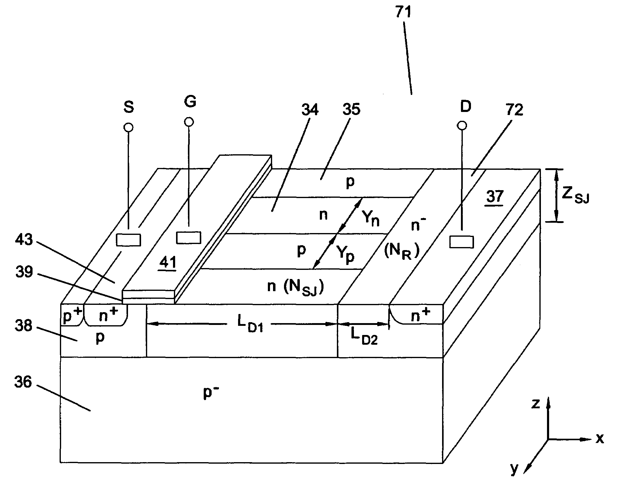
[0025]A preferred embodiment of the present invention is illustrated in FIG. 7. The formation of the SJR-LDMOST 70 preferably includes the deposit of an epitaxial layer 72 on a substrate 36, where the epitaxial layer 72 has a doping polarity opposite to that of the substrate 36. In the embodiment shown in FIG. 7, a p− substrate 36 is used in conjunction with an n− epitaxial layer 72. The thickness of the epitaxial layer 72 is ZSJ. An n+ drain region 37 is formed in a portion of the epitaxial layer 72 and a p-well region 38 is formed in another portion of the epitaxial layer 72 separate from the n+ drain region 37. An n+ source region 43 is formed within the p-well region 38. A gate region consisting of a thin oxide layer 39 covered with a gate electrode 41 straddles the p-well region 38. In operation, an inversion layer forms a channel at the surface of the p-well region 38 to allow current to flow between the n+ source region 43 and n+ drain region 37 when an appropriate control si...


PUM


Abstract

A lateral double diffused MOSFET (LDMOST) incorporates both the reduced surface field (RESURF) and super junction (SJ) in a split-drift region to significantly improve the on-state, off-state and switching characteristics in junction-isolated (JI) technology. The structure effectively suppresses substrate-assisted-depletion which is the main problem encountered when applying the SJ concept to lateral power devices. The device structure features a split-drift region formed of two parts: a SJ structure that extends over most of the drift region, and a terminating RESURF region occupying a portion of the drift region next to the drain. The structure offers improved breakdown voltage and reduced specific on resistance as compared to convention structures, and is useful in power integrated circuits suitable for a variety of applications including flat plasma panel display, automotive electronics, motor control, power supply and high voltage lamp ballasts.

Description

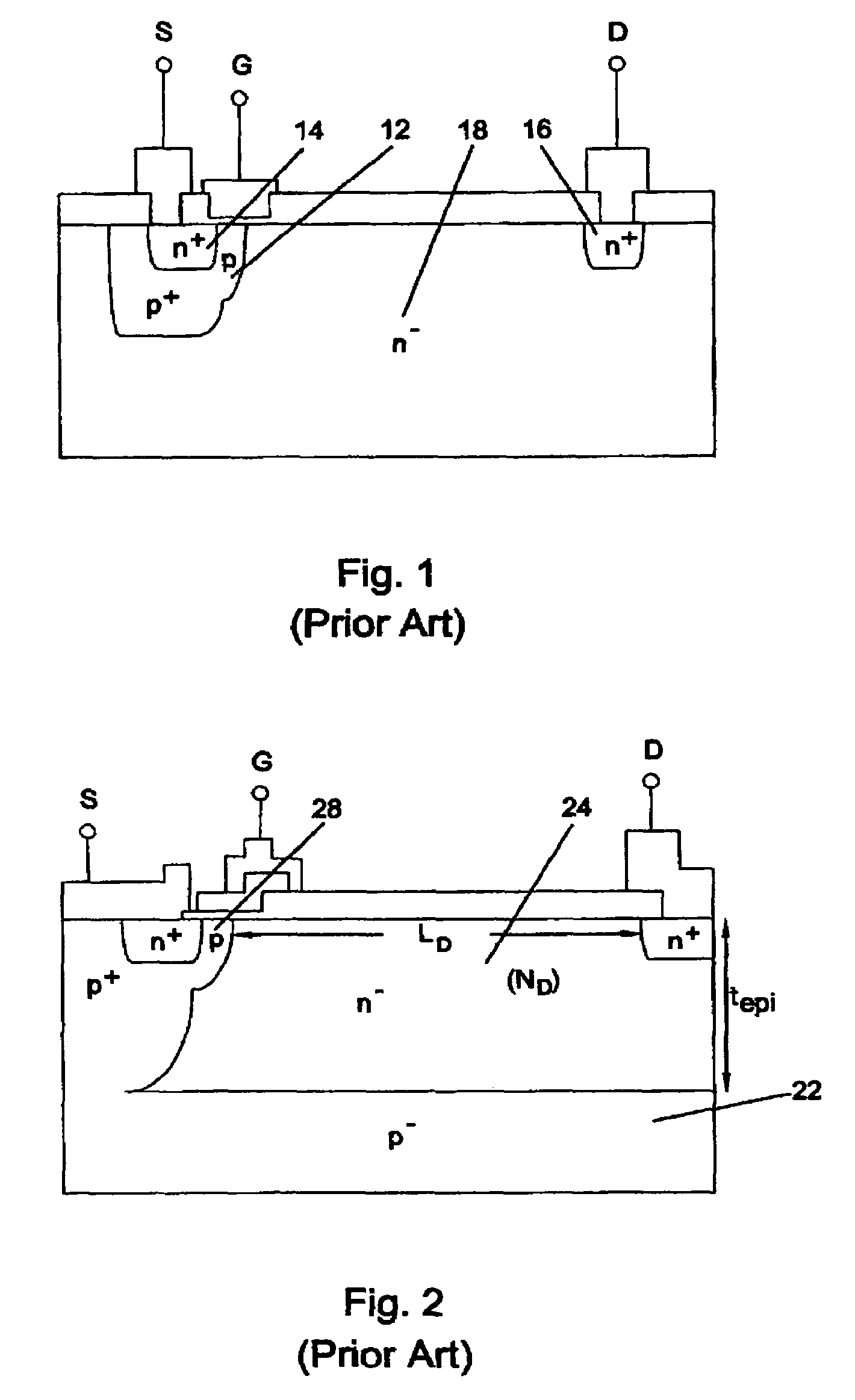
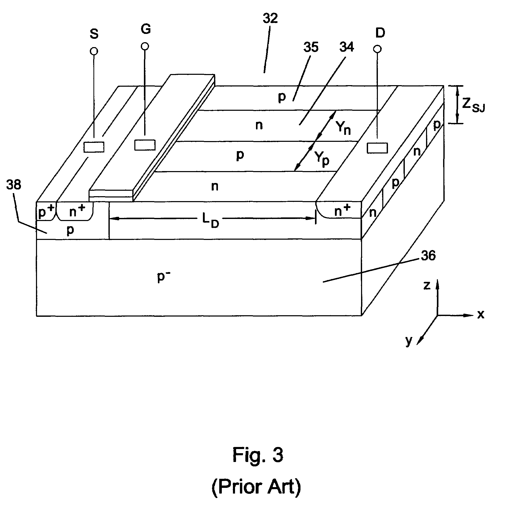
BACKGROUND OF INVENTION[0001]The present invention relates to semiconductor devices, and in particular to Lateral Double Diffused MOSFET (LDMOST) semiconductor devices.[0002]In a conventional LDMOST, a well region and a source region are typically created via a double diffusion process or ion-implantation process by which the well region and source region are formed through a common opening window that is self-aligned to a gate. This technique facilitates control of the lateral diffusion of the impurities under the gate so that small channel lengths can be realized without the use of high-resolution photolithography. An example of a conventional n-well LDMOST 10 is illustrated in FIG. 1, and includes a p-well region 12 and an n+ drain region 16 formed in an n− substrate 18. An n+ source region 14 is formed within the p-well region 12. Current flows laterally from the source region 14 to the drain region 16, when an applicable control voltage is applied to the gate to form a channel ...

Claims


Application Information

Patent Timeline
Patent Type & Authority Patents(United States)
IPC IPC(8): H01L29/76H01L29/94H01L31/062H01L31/119H01L29/06H01L29/417H01L29/423H01L29/78
CPCH01L29/0634H01L29/7801H01L29/42368H01L29/41758H01L29/402H01L29/0878H01L29/7816
Inventor SALAMA, C. ANDRE T.NASSIF, SAMEH KHALIL
Owner SALAMA C ANDRE T
Learn More