
Nitride semiconductor light-emitting device with electrode pattern

a technology of semiconductor light-emitting devices and semiconductors, which is applied in the direction of semiconductor devices, basic electric elements, electrical appliances, etc., can solve the problems of ineffective active layers and difficult processing, and achieve the effect of improving current spreading

Inactive Publication Date: 2009-06-25
SAMSUNG ELECTRONICS CO LTD
View PDF14 Cites 67 Cited by
  • Summary
  • Abstract
  • Description
  • Claims
  • Application Information

AI Technical Summary

Benefits of technology

[0014]An aspect of the present invention provides a nitride semiconductor light-emitting device with an electrode pattern that improves current spreading to an active layer.
[0015]According to an aspect of the present invention, there is provided a nitride semiconductor light-emitting device with multiple layers of a substrate, an n-type nitride layer, an active layer of a multi-quantum-well structure, and a p-type nitride layer, the nitride semiconductor light-emitting device including: a p-electrode pattern including one or more p-pads disposed on the p-type nitride layer, and one or more p-fingers extending from the p-pads; and an n-electrode pattern including one or more n-pads disposed on an exposed region of the n-type nitride layer to correspond to the p-pads, and one or more n-fingers extending from the n-pads, wherein the n-fingers have identical resistance, and the p-fingers have identical resistance to improve current spreading to the active layer.

Problems solved by technology

However, these approaches have certain limitations that lead to processing difficulties.
However, decreasing the size of the n-electrode is accompanied by an increased driving voltage and a reduced current spreading effect, which can render the active layer for emitting light useless.

Method used


Image

  • Nitride semiconductor light-emitting device with electrode pattern
  • Nitride semiconductor light-emitting device with electrode pattern
  • Nitride semiconductor light-emitting device with electrode pattern

Examples


Embodiment Construction

[0033]Exemplary embodiments of the present invention will now be described in detail with reference to the accompanying drawings.

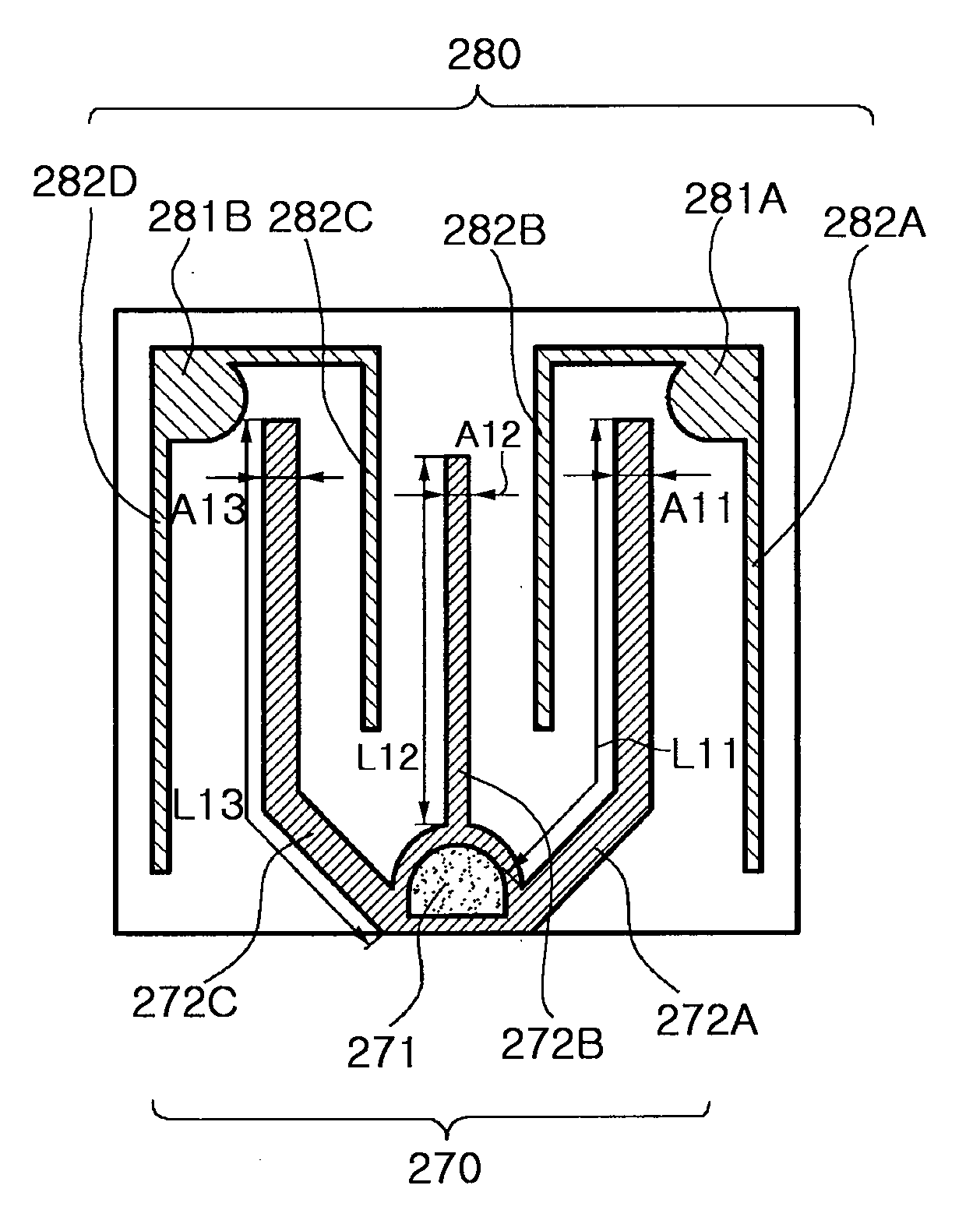
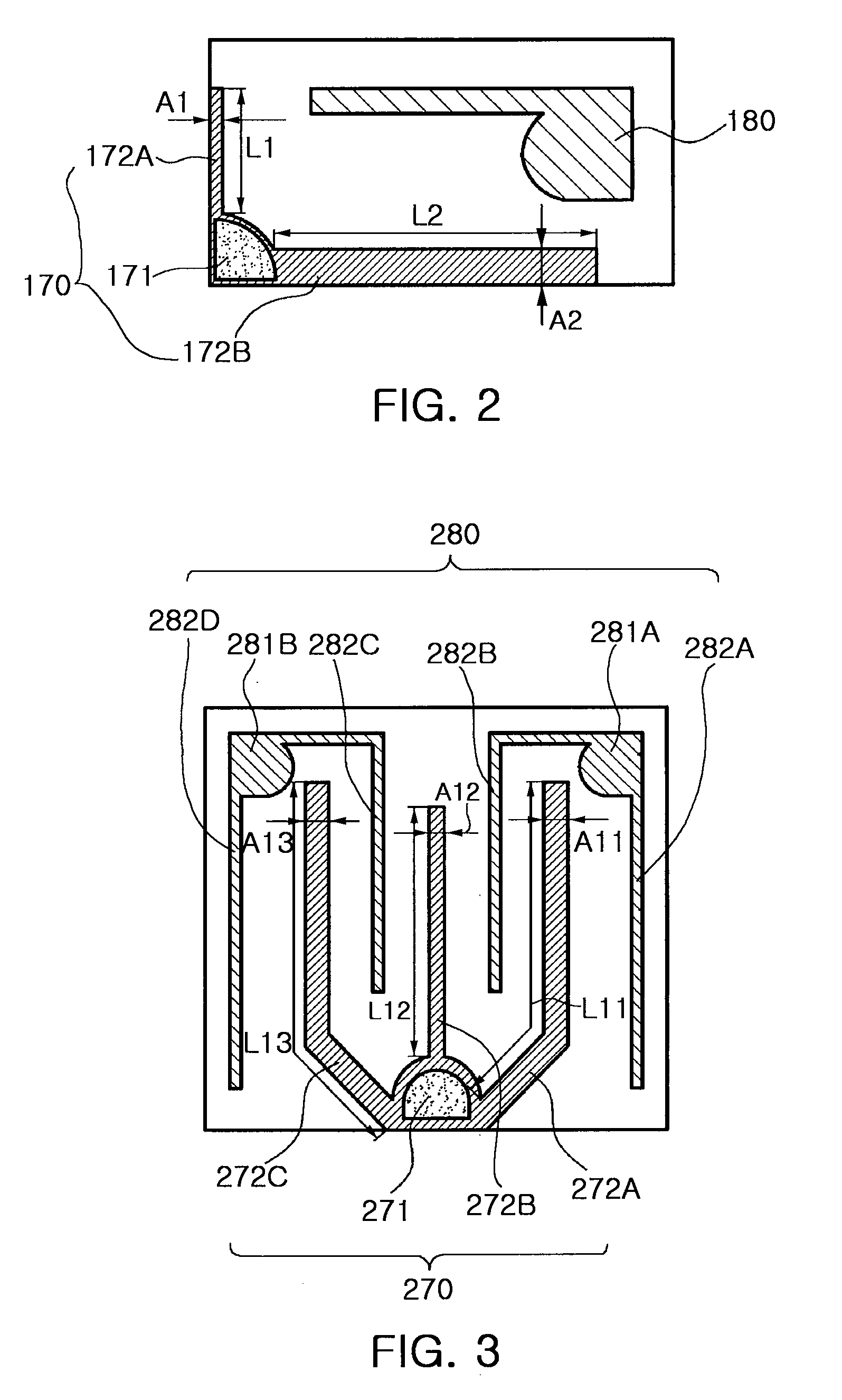
[0034]FIG. 2 is a schematic view of electrode patterns of a horizontal type nitride semiconductor light-emitting device according to an embodiment of the present invention. FIG. 2 illustrates a p-electrode pattern disposed on a p-type nitride layer (not shown) and an n-electrode pattern disposed on an exposed region of an n-type nitride layer in a horizontal type nitride semiconductor light-emitting device. Here, well-known configurations or functions of the nitride semiconductor light-emitting device will not be described in detail when they would obscure the subject matter of the invention.

[0035]Referring to FIG. 2, the horizontal type nitride semiconductor light-emitting device may include the p-electrode pattern 180 and the n-electrode pattern 170. The p-electrode pattern 180 may be disposed on the p-type nitride layer (not shown). The n-electrode patt...


PUM


Abstract

A nitride semiconductor light-emitting device with an electron pattern that applies current uniformly to an active layer to improve light emission efficiency is provided. The nitride semiconductor light-emitting device includes multiple layers of a substrate, an n-type nitride layer, an active layer of a multi-quantum-well structure, and a p-type nitride layer. The nitride semiconductor light-emitting device further includes a p-electrode pattern and an n-electrode pattern. The p-electrode pattern includes one or more p-pads disposed on the p-type nitride layer, and one or more p-fingers extending from the p-pads. The n-electrode pattern includes one or more n-pads disposed on an exposed region of the n-type nitride layer to correspond to the p-pads, and one or more n-fingers extending from the n-pads. The n-fingers have identical resistance, and the p-fingers have identical resistance to improve current spreading to the active layer.

Description

CROSS-REFERENCE TO RELATED APPLICATIONS[0001]This application claims the priority of Korean Patent Application No. 2007-134581 filed on Dec. 20, 2007, in the Korean Intellectual Property Office, the disclosure of which is incorporated herein by reference.BACKGROUND OF THE INVENTION[0002]1. Field of the Invention[0003]The present invention relates to a nitride semiconductor light-emitting device, and more particularly, to a nitride semiconductor light-emitting device with an electron pattern that applies current uniformly to an active layer to improve light emission efficiency.[0004]2. Description of the Related Art[0005]A light-emitting diode (LED) is a nitride semiconductor light-emitting device that emits light by recombination of electrons and holes. LEDs are widely used as light sources in optical communication devices, electronic devices, and the like.[0006]In an LED, the frequency (or wavelength) of emitted light is a function of a band gap of a material of the semiconductor d...

Claims


Application Information

Patent Timeline
Patent Type & Authority Applications(United States)
IPC IPC(8): H01L33/00H01L33/32H01L33/38
CPCH01L33/20H01L33/38H01L33/32
Inventor LEE, JIN BOCKKIM, DONG WOOHNYOON, SANG HOCHOI, PUN JAE
Owner SAMSUNG ELECTRONICS CO LTD
Features
  • Generate Ideas
  • Intellectual Property
  • Life Sciences
  • Materials
  • Tech Scout
  • Unparalleled Data Quality
  • Higher Quality Content
  • 60% Fewer Hallucinations
Learn More