Passive Fourier Transform Circuits and Butler Matrices

a fourier transform circuit and butler matrix technology, applied in the field of radio frequency circuits, filters, mobile communications network stations, satellites, etc., can solve the problems of a small, battery-powered device such as a cellphone, the frequency with which ffts of this size are processed, and the computational burden of ffts of this size is significant, so as to reduce throughput losses

Active Publication Date: 2009-06-25
TELEFON AB LM ERICSSON (PUBL)
View PDF6 Cites 38 Cited by
  • Summary
  • Abstract
  • Description
  • Claims
  • Application Information

AI Technical Summary

Benefits of technology

[0010]According to another exemplary embodiment, the coupling circuit described herein may combine a transceiver bandpass filtering function with a Butler matrix operation. In so doing, this embodiment eliminates the need for both a Butler matrix circuit and a filter circuit between a transceiver and an antenna, which reduces throughput losses between the transceiver and antenna. For this embodiment, a resonator circuit is connected to each of multiple ones of the inputs and outputs. Each resonator circuit comprise a shunt inductor, a series inductor, an inductor-capacitor combination, a coaxial resonator, and / or a surface acoustic wave resonator. Each resonator circuit is configured to adapt the frequency response of the coupling circuit such that the coupling circuit has a bandpass frequency response comprising a desired bandwidth around a desired center frequency.

Problems solved by technology

In these early implementations, even an FFT of size 32 was a significant digital signal processing computational burden, because of the embryo state of digital integrated circuits.
Today, the proposed sizes of FFT for future OFDM systems is of the order of 1024-4096, and while modern digital signal processors have advanced significantly in speed and performance, the frequency with which FFTs of this size must be performed, such as every 63.5 microseconds in one proposal, is still a burden for a small, battery-powered device such as a cellphone.
FFT decomposition reduces the number of arithmetic operations in a digital algorithm, and therefore the complexity.
The inputs to the coupling circuit may have balanced or unbalanced quadriphase input signals.

Method used


Image

  • Passive Fourier Transform Circuits and Butler Matrices
  • Passive Fourier Transform Circuits and Butler Matrices
  • Passive Fourier Transform Circuits and Butler Matrices

Examples


Embodiment Construction

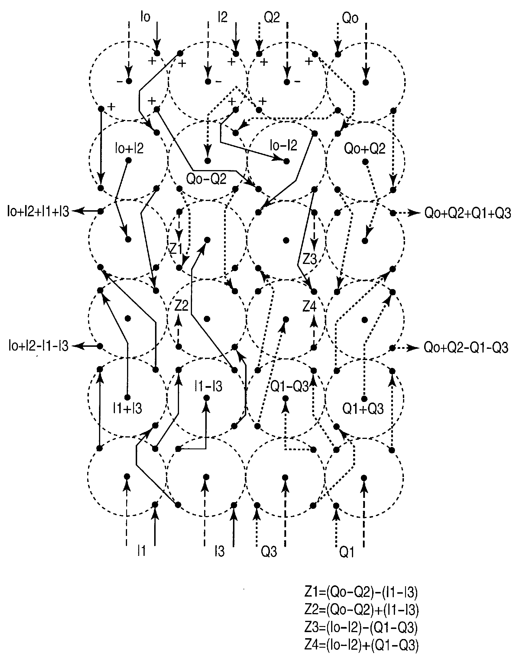
[0049]A coupling circuit according to the present invention comprises passive analog components for coupling a transceiver to an antenna, such as an antenna array. The coupling circuit transforms an input signal into an appropriate format for each element of the antenna array to perform a Discrete Fourier Transform (DFT) on the input signal, a Fast Fourier Transform (FFT) on the input signal, and / or to implement a Butler matrix.

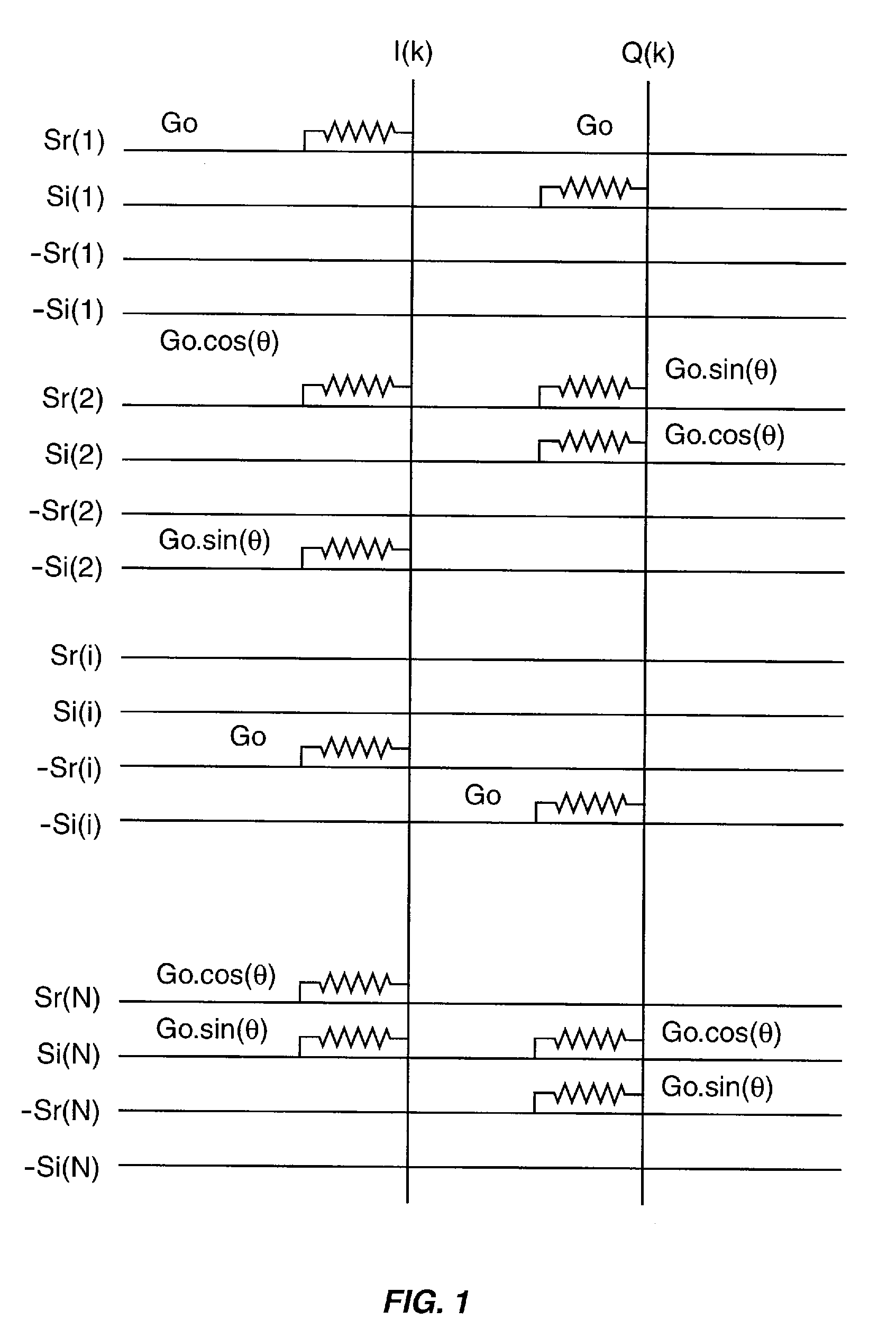
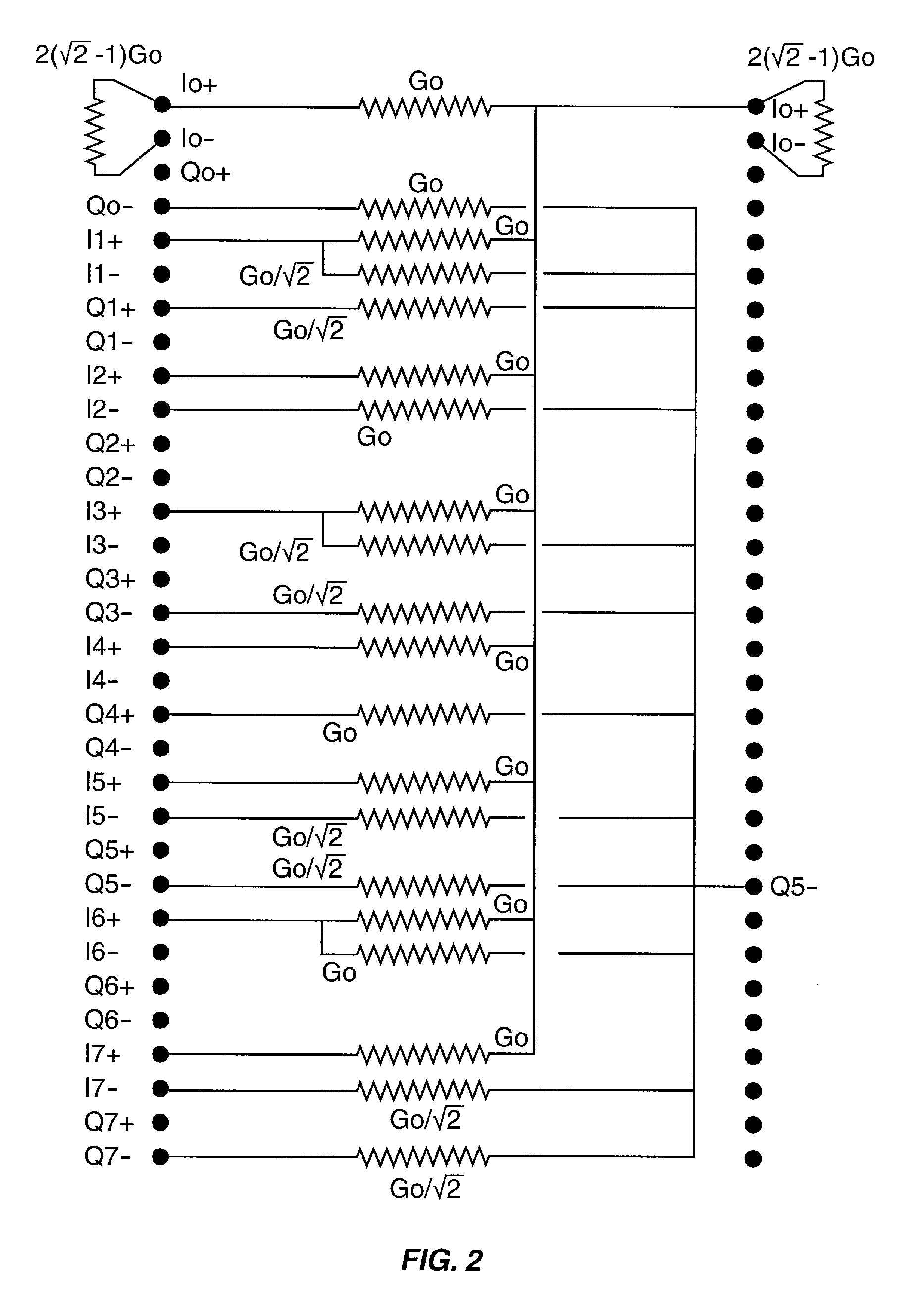
[0050]The coupling circuit comprises a coupling network having a plurality of inputs and a plurality of outputs, where the inputs provide quadriphase versions of at least one input signal. The quadriphase versions include positive (non-phase-inverted) and negative (phase-inverted) In-phase (I) or real signals, respectively designated as I+ and I−, and positive and negative Quadrature (Q) signals, respectively designated as Q+ and Q−. The outputs of the coupling network are coupled to one or more of the I+, I−, Q+, and Q− signals such that a desired phase shif...


PUM


Abstract

The coupling circuit described herein comprises passive analog components for coupling a transceiver to an antenna, such as an antenna array. The coupling circuit transforms an input signal into an appropriate format for each element of the antenna array. The coupling circuit comprises a coupling network having a plurality of inputs and a plurality of outputs. The inputs provide quadriphase versions of at least one input signal. In one embodiment, the coupling circuit performs a Discrete Fourier Transform (DFT) on the input signal. In another embodiment, the coupling circuit performs a Fast Fourier Transform (FFT) on the input signal. In still another embodiment, the FFT performed by the coupling circuit implements a Butler matrix.

Description

BACKGROUND OF THE INVENTION[0001]The present invention generally relates to the field of radio frequency circuits, filters, antenna beamforming, mobile communications network stations, and satellites, and more particularly relates to analog implementations of circuits that couple transceivers to antennas.[0002]Orthogonal Frequency Division Multiplex (OFDM) and Orthogonal Frequency Division Multiple Access (OFDMA) are digital data communications techniques that originated before the 1970's as a method of transmitting data over HF Ionosphere radio paths and are enjoying a new resurgence in connection with possible future public wireless communications systems.[0003]Early OFDM system were known variously as multi-tone modems or Kineplex, and divided a data stream for transmission into perhaps 32 low data rate streams, which were each modulated onto one of 32 orthogonally spaced subcarriers. The generation of 32 modulated carriers was carried out by applying 32 symbol-representative sig...

Claims


Application Information

Patent Timeline
Patent Type & Authority Applications(United States)
IPC IPC(8): H03H7/21G06F17/14
CPCH01Q3/40H04B1/0458H01Q25/007
Inventor DENT, PAUL WILKINSON
Owner TELEFON AB LM ERICSSON (PUBL)
Why Eureka
Try Eureka