Magnetic device

a magnetic device and insulating layer technology, applied in the direction of transformers/inductance coils/windings/connections, using reradiation, instruments, etc., can solve the problems of increasing the variation of noise restraining ability, scratching the insulating layer of enameled wires, and the winding distribution of wires may be non-uniform, so as to reduce the affection of magnetic devices, reduce manufacturing costs, and eliminate winding variations

Inactive Publication Date: 2009-06-25
DELTA ELECTRONICS INC
View PDF10 Cites 32 Cited by
  • Summary
  • Abstract
  • Description
  • Claims
  • Application Information

AI Technical Summary

Benefits of technology

[0011]As mentioned above, the magnetic device of the present invention includes a plurality of conductive wire segments instead of the conventional single wire. The conductive wire segments are wound around the magnetic induction element and the insulating structure, and the ends of the conductive wire segments are electrically connected to the conductive layer of the circuit board to form a coil loop. Compared with the prior art, the present invention can carry out the automatic

Problems solved by technology

However, this may scratch the insulating layer of the enameled wires 13.
In addition, the winding distribution of the wires may be non-uniform due to the different winding methods and directions.
Therefore, the stray capacitance of the inductor becomes

Method used


Image

  • Magnetic device
  • Magnetic device
  • Magnetic device

Examples


first embodiment

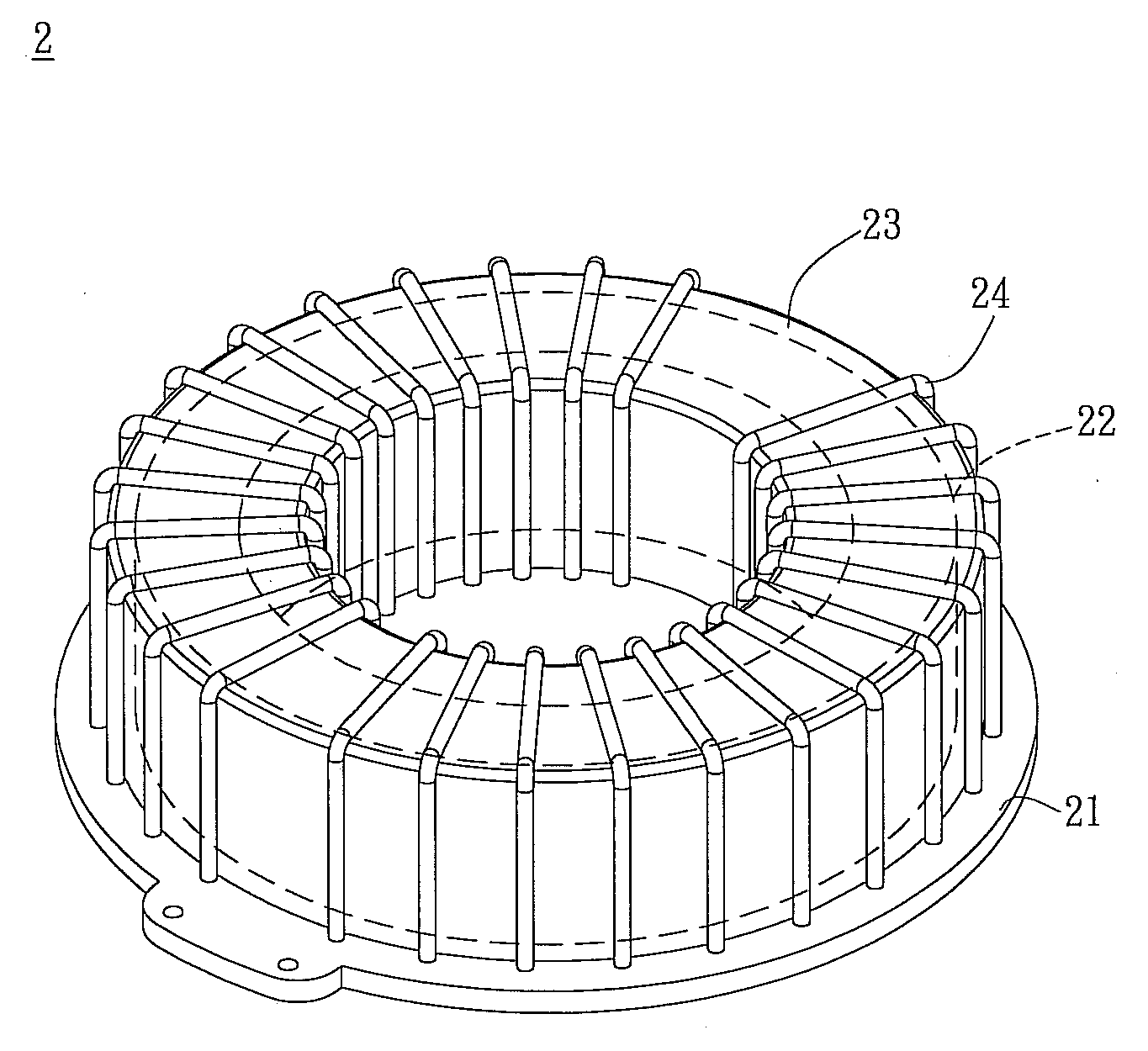
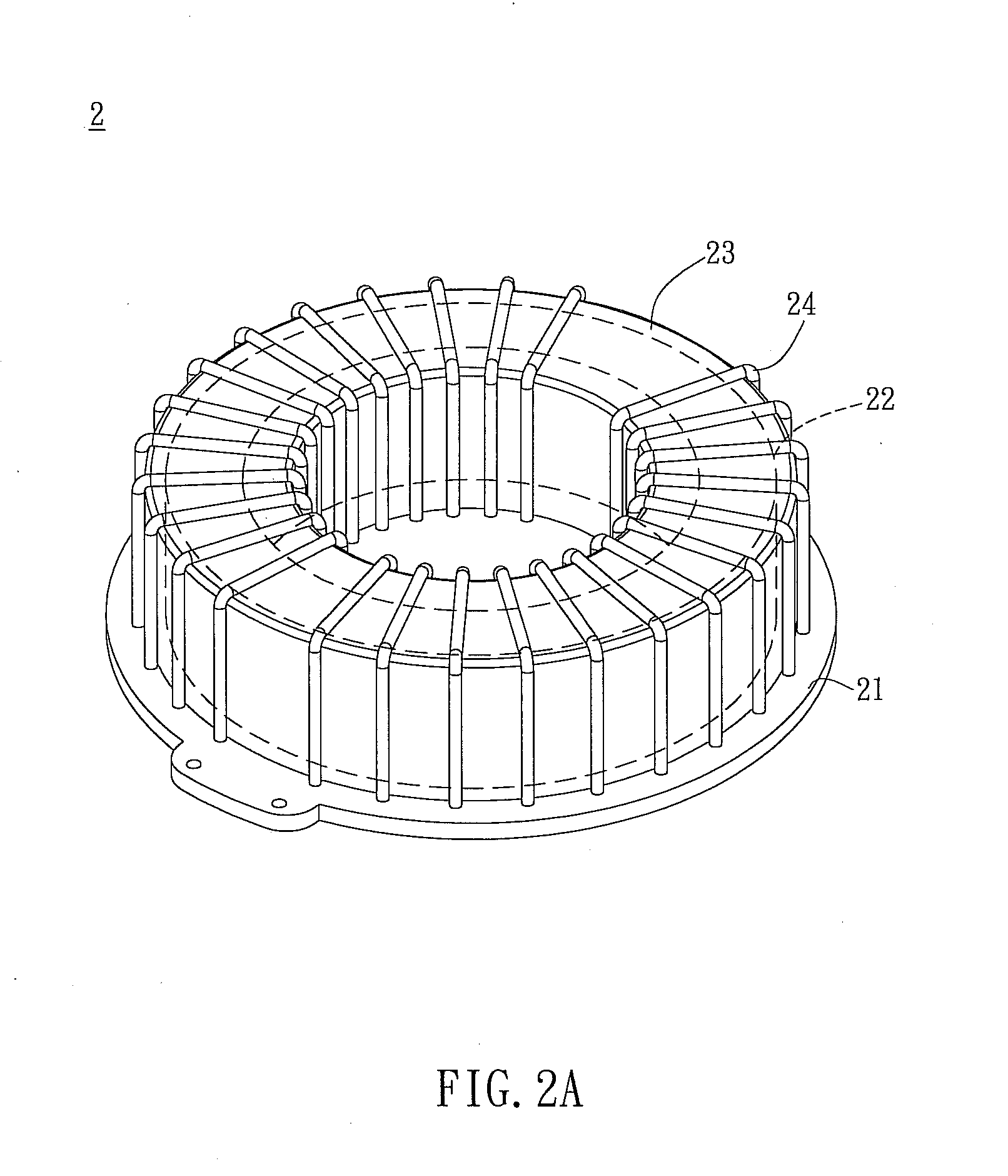
[0025]With reference toFIGS. 2A to 2D, a composite inductor 2 according to a first embodiment of the present invention includes a circuit board 21, a magnetic induction element 22, an insulating structure 23 and a plurality of conductive wire segments 24. The circuit board 21 can be a printed circuit board and includes at least one conductive layer 211 as shown in FIG. 2C. The material of the conductive layer 211 includes gold, silver, copper, tin or alloys thereof. In the embodiment, the conductive layer 211 is, for example but not limited to, a copper layer.

[0026]For example, the magnetic induction element 22 is annular, elliptic or rectangular, and the material of the magnetic induction element 22 includes iron, cobalt, nickel or alloys thereof. In the embodiment, the magnetic induction element 22 is an annular iron core and is disposed on the circuit board 21. The insulating structure 23 is, for example but not limited to, an insulating housing for covering the magnetic inductio...

second embodiment

[0029]With reference to FIG. 3, a composite inductor 3 according to a second embodiment of the present invention includes a circuit board 31, a magnetic induction element 22, an insulating structure 23 and a plurality of conductive wire segments 34.

[0030]The different between the composite inductors 2 and 3 is in that the conductive wire segments 34 of the composite inductor 3 are disposed on the circuit board 31, which has a plurality of conductive layers 311. In the embodiment, two ends of each conductive wire segment can be disposed on different conductive layers, respectively (not shown). The conductive wire segments 34 are electrically connected to the conductive layers 311 to form a coil. Accordingly, the current durability of the composite inductor 3 can be increased by the increased area of the total conductive layers 311.

third embodiment

[0031]With reference to FIG. 4, a composite inductor 4 according to a third embodiment of the present invention includes a circuit board 41, a magnetic induction element 22, an insulating structure 23, a plurality of conductive wire segments 44 and a plurality of conductive wire segments 45.

[0032]The difference between the composite inductors 4 and 2 is in that the conductive wire segments 44 and 45 of the composite inductor 4 are disposed on the circuit board 41, which has a plurality of conductive layers 411 and 412. In the embodiment, the number of the conductive wire segments 44 is the same as that of the conductive wire segments 24 of the first embodiment, and the conductive wire segments 45 are newly added. The conductive wire segments 411 and 412 are connected to each other through at least one via (not shown), so that the conductive wire segments 44 and 45 can be electrically connected to the conductive layers 411 and 412 so as to form a coil. Accordingly, the winding densit...


PUM


Abstract

A magnetic device includes a circuit board, a magnetic induction element, an insulating structure and a plurality of conductive wire segments. The circuit board has at least one conductive layer. The magnetic induction element is disposed on the circuit board. The insulating structure covers the magnetic induction element. The insulating structure is wound by the conductive wire segments. Two ends of each conductive wire segments are electrically connected to the conductive layer to form a coil loop.

Description

CROSS REFERENCE TO RELATED APPLICATIONS[0001]This Non-provisional application claims priority under 35 U.S.C. §119(a) on Patent Application No(s). 096148596 filed in Taiwan, Republic of China on Dec. 19, 2007, the entire contents of which are hereby incorporated by reference.BACKGROUND OF THE INVENTION[0002]1. Field of Invention[0003]The present invention relates to a magnetic device such as an inductor, a filter or a transformer.[0004]2. Related Art[0005]Taking the conventional inductor as an example, it is usually made by directly winding an enameled wire on a material with the magnetic induction property. When the current is applied to the inductor, the inductance can be obtained. As shown in FIG. 1, a conventional inductor 1 includes an insulating housing 11, an iron core 12 and two enameled wires 13. The iron core 12 is an annular iron core, and the insulating housing 11 covers the iron core 12. The enameled wires 13 are wound on the iron core 12 by hand or machine.[0006]In the...

Claims


Application Information

Patent Timeline
IPC IPC(8): H01F27/30H01F27/36H01F27/29
CPCH01F27/2804H01F2027/2814H01F27/306H01F27/2895
Inventor YANG, CHUNG-JUNGKUNG, CHUAN-YUANCHEN, MAN-MEITSAI, PO-JEN
Owner DELTA ELECTRONICS INC
Why Eureka
Try Eureka