Nitride Semiconductor Light Emitting Device

a light-emitting device and nitride technology, applied in the direction of solid-state devices, semiconductor lasers, lasers, etc., can solve the problems of reducing light-emitting efficiency, unable to obtain semiconductor light-emitting devices with high efficiency, and enhancing light-emitting efficiency so high as a theoretical value, etc., to achieve high luminance efficiency, high efficiency, and low cost

Inactive Publication Date: 2009-07-02
ROHM CO LTD
View PDF2 Cites 40 Cited by
  • Summary
  • Abstract
  • Description
  • Claims
  • Application Information

AI Technical Summary

Benefits of technology

[0014]According to the present invention, since the thin film barrier layer having a larger band gap energy than that of the well layer is provided within the well layer, the well layer is divided into at least the first well layer and the second well layer by the thin film barrier layer, a barrier effect against electrons and holes is generated by the thin film barrier layer, the electrons and the holes approach each other at the first well layer and the second well layer interposing the thin film barrier layer, and, as a result, recombination radiation can be accelerated between the electrons and the holes existing in the first well layer and the second well layer divided.
[0015]In addition, since a thickness of the thin film barrier layer is set 20 Angstroms or less, a function of the well layer is not spoiled by imposing of the thin film barrier layer, and an effect of a conventional well layer can be maintained. Therefore, a semiconductor light emitting device with significantly high luminance efficiency can be obtained comparing to that in case of using a usual MQW active layer. In addition, in case of forming a light emitting device such as a green or yellow LED in which a thickness of a well layer is large, luminance efficiency never lowers. As a result, even if a LED, LD or the like emitting ultraviolet to yellow light, a semiconductor light emitting device with high characteristics having high internal quantum efficiency and a low threshold current can be obtained.

Problems solved by technology

However, even if a device is actually manufactured by employing an active layer having a multi quantum well structure made of nitride semiconductor, there is a problem such that light emitting efficiency can not be enhanced so high as a theoretical value.
However, if the composition of In of the active layer is increased, since In is unevenly distributed in the active layer, a desired wavelength can not be obtained, and crystallinity is deteriorated by increasing of the composition of In, and then light emitting efficiency is lowered corresponding to lengthening a wavelength.
However, if a thickness of the well layer is increased, light emitting efficiency can not be enhanced so high as a theoretical value as described above, and it is more noticeable than in case of a short wavelength semiconductor light emitting device of blue or ultraviolet light, then there arises a problem such that a semiconductor light emitting device with high efficiency can not be obtained.

Method used


Image

  • Nitride Semiconductor Light Emitting Device
  • Nitride Semiconductor Light Emitting Device
  • Nitride Semiconductor Light Emitting Device

Examples


Embodiment Construction

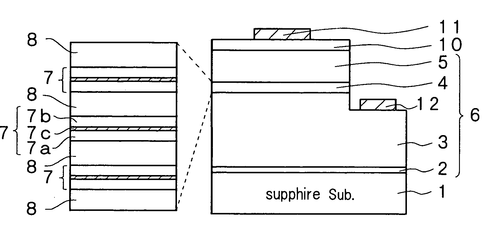
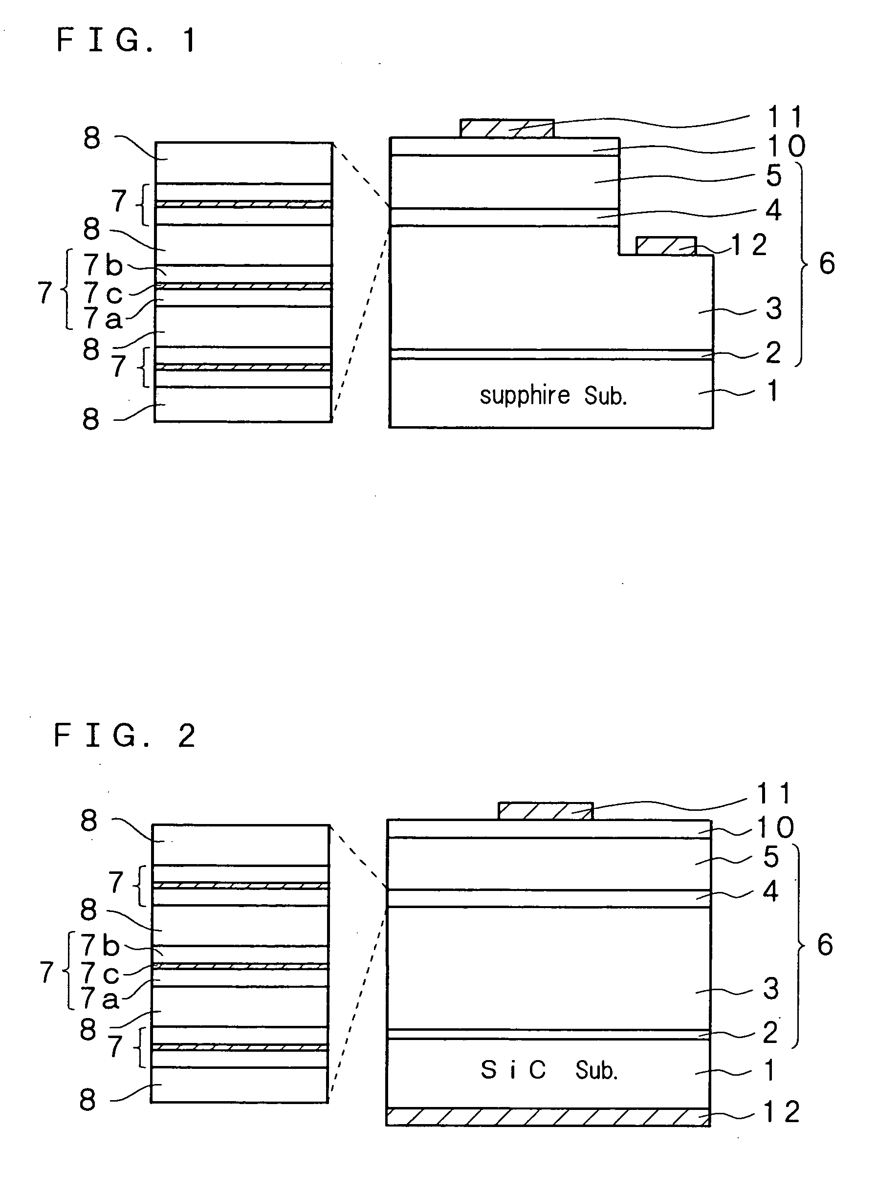
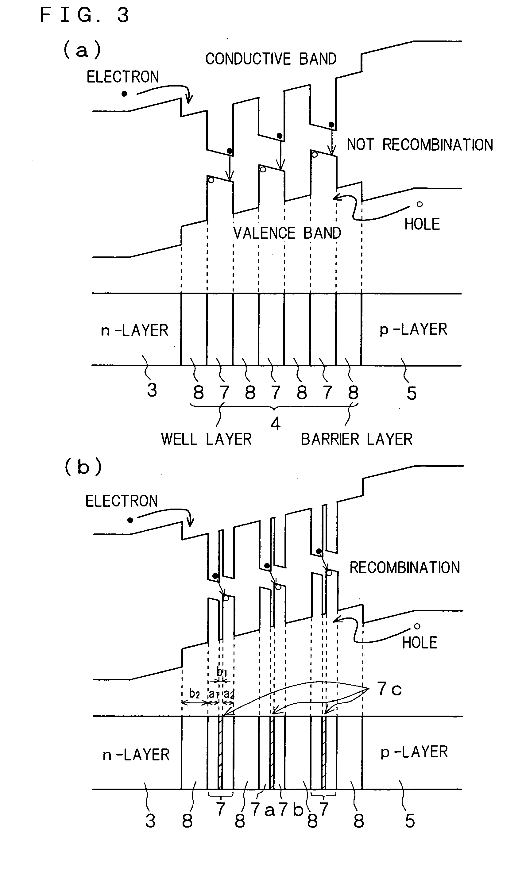
[0030]An explanation will be given below of a nitride semiconductor light emitting device according to the present invention in reference to the drawings. As an explanatory cross-sectional view of the nitride semiconductor light emitting device (LED chip) of an embodiment is shown in FIG. 1, the nitride semiconductor light emitting device according to the present invention is provided with a nitride semiconductor lamination portion 6 provided on a substrate 1. The nitride semiconductor lamination portion 6 includes at least an active layer 4 in which a light emitting portion is formed. And the active layer 4 is constituted with a multiple quantum well structure formed by laminating well layers 7 made of InxGa1-x N (08 made of AlyInzGa1-y-zN (0≦y7 is divided at least into a first well layer 7a and a second well layer 7b by a thin film barrier layer 7c made of AlvInwGa1-v-wN (0≦v7c is formed so as to have a thickness of one atomic layer or more and 20 Angstroms or less. In addition, s...


PUM


Abstract

There is provided a nitride semiconductor light emitting device having high internal quantum efficiency by accelerating recombination radiation while employing a multiple quantum well structure in which each of well layers has a relatively large thickness. The nitride semiconductor light emitting device is provided with a nitride semiconductor lamination portion (6) provided on a substrate (1). The nitride semiconductor lamination portion (6) includes at least an active layer (4) in which a light emitting portion is formed. And the active layer is constituted with a multiple quantum well structure formed by laminating well layers (7) made of InxGa1-xN (0<x≦1), and barrier layers (8) made of AlyInzGa1-y-zN (0≦y<1, 0≦z<1, 0≦y+z<1, z<x) alternately. In addition, one of the well layers is divided at least into a first well layer (7a) and a second well layer (7b) by a thin film barrier layer (7c) made of AlvInwGa1-v-wN (0≦v<1, 0≦w<1, 0≦v+w<1, w<x), and the thin film barrier layer is formed so as to have a thickness of one atomic layer or more and 20 Angstroms or less.

Description

FIELD OF THE INVENTION[0001]The present invention relates to a semiconductor light emitting device using nitride semiconductor, such as a light emitting device like a light emitting diode (LED), a laser diode (LD) or the like. More particularly, the present invention relates to a nitride semiconductor light emitting device capable of realizing low threshold current and low driving current and voltage operation, by enhancing light emitting efficiency at a well layer composing an active layer in a semiconductor light emitting device having an active layer with a multi quantum well structure.BACKGROUND OF THE INVENTION[0002]In recent years, nitride semiconductor light emitting devices such as a blue light emitting diode (LED), a laser diode or the like, using nitride semiconductor, have been in practical use, and here a multi quantum well structure is employed in order to enhance light emitting efficiency at an active layer to achieve high luminance and high output. As shown, for examp...

Claims


Application Information

Patent Timeline
Patent Type & Authority Applications(United States)
IPC IPC(8): H01L33/00H01L33/06H01L33/32H01L33/42
CPCB82Y20/00H01L33/06H01S5/34333H01S5/3407H01S5/3408H01L33/32
Inventor SHAKUDA, YUKIO
Owner ROHM CO LTD
Why Eureka
Try Eureka