Thick film resistor

a resistor and film technology, applied in the direction of resistors, resistive elements, adjustable resistors, etc., can solve the problem of resistor negatively affecting a noise characteristic, and achieve excellent noise characteristics and high potential distribution stability

Inactive Publication Date: 2009-07-09
HITACHI HIGH-TECH CORP +1
View PDF6 Cites 7 Cited by
  • Summary
  • Abstract
  • Description
  • Claims
  • Application Information

AI Technical Summary

Benefits of technology

[0013]According to the present invention, it is possible to design a wiring pattern having a uniform potential gradient. Therefore, since the thick film resistor has high stability in potential distribution and variation of stray capacitance around the resistor in addition to an insulation performance, it is possible to form a thick film resistor having an excellent noise characteristic.

Problems solved by technology

Since nonuniformity of the potential gradient in the resistor requires the high insulation performance and may be sensitively influenced by potential distribution and variation of stray capacitance around the resistor, the nonuniformity of the potential gradient in the resistor negatively influences a noise characteristic.

Method used


Image

  • Thick film resistor
  • Thick film resistor
  • Thick film resistor

Examples


first embodiment

of Resistor

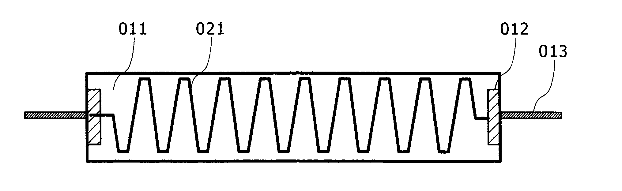
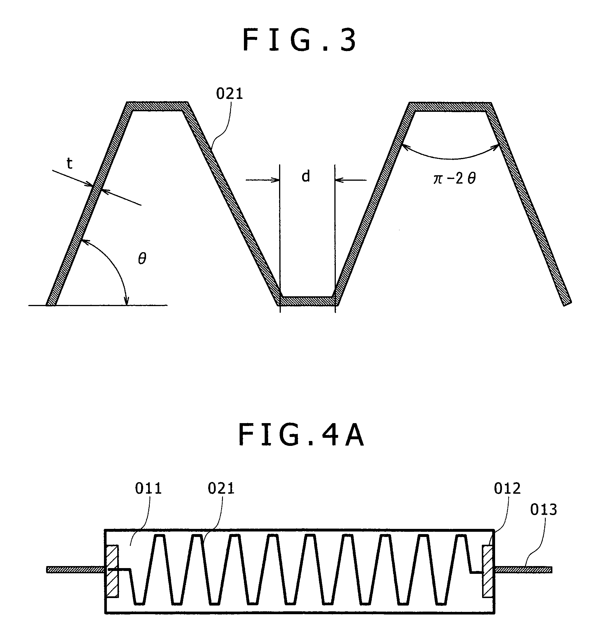
[0038]FIG. 4A is a schematic diagram of a thick film resistor having a zigzagged wiring pattern according to a first embodiment of the present invention. In the case of a flat plate type thick film resistor, since a wiring pattern of a resistance wire 021 is sintered by screen printing after electrode conductors 012 that face each other are formed on an insulating substrate 011, there is no problem in manufacturing a thick film resistor as shown in FIG. 4A when a mask for the screen printing is designed to satisfy Expression 1.

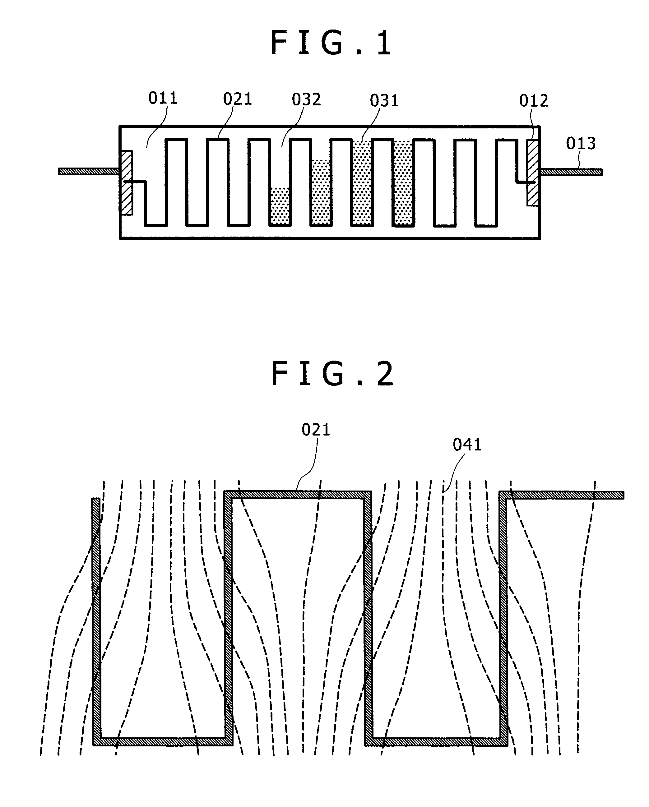
[0039]FIG. 4B illustrates a state of an equipotential line on a plane where a resistance wire is disposed. In FIG. 2, the spacing between the equipotential lines is narrowed outside the bent section of the resistance wire, but in FIG. 4B, the spacing between the equipotential lines is widened outside of the bend section by properly selecting a bending angle and as a result, the equipotential lines 041 become parallel to each other. That is, it can b...

second embodiment

of Resistor

[0041]The resistivity of the thick film resistor slightly varies depending on the mixing, the sintering temperature, etc. of a paste material used for the resistance wire. Therefore, it is difficult to accurately match a final resistance value with a predetermined value only by designing the geometrical shape of the resistance wire. As a method of adjusting the above, a trimming process to mechanically correct a partial shape of the resistance wire has to be necessarily performed. In general, laser irradiation or sandblasting can be used for the trimming process. However, the laser irradiation and the sandblasting are the same as each other in that parts of all the resistors are cut and removed.

[0042]Even in the thick film resistor according to the second embodiment of the present invention, the trimming process is considered to be necessarily in practical use performed. It is preferable that the used trimming method maintains the shape that satisfies Expression 1 in orde...

third embodiment

of Resistor

[0043]FIG. 6 illustrates an example of a case that a resistor according to the present invention and a resistor for adjusting a resistance value by the trimming process are formed on the same insulating substrate. In this example, since the two resistors are connected to each other in series, the two resistors share one electrode. The resistor of the present invention and the resistor for adjusting the resistance value may be separately connected to the electrode and plural resistors may be connected to the electrode so that a combined resistance value becomes a predetermined resistance value after the two resistors are manufactured as completely different components. At this time, the resistor of the present invention takes charge of a main function of the resistance value and the other resistor takes charge of adjusting the final resistance value.


PUM


Abstract

In a flat plate type thick film resistor, an insulation performance is improved by excluding the nonuniformity of potential distribution on a wiring plane, which is generated when electric current flows in a resistance wire. Simultaneously, generation of noise depending on potential distribution and variation of stray capacitance around a resistor is suppressed. When the resistance wire having a constant thickness and uniform resistivity, which is formed on an insulating substrate, is connected to a pair electrode conductors that face to each other, in the way that the resistance wire is repetitively bent to the alternate side in zigzags, a potential gradient on the wiring plane, which is generated when electric current flows in the resistance wire, is constant by properly selecting the line width, the bending angle, and the spacing between bending vertexes of a resistance wire.

Description

CLAIM OF PRIORITY[0001]The present application claims priority from Japanese patent application JP2007-330388 filed on Dec. 21, 2007, the content of which is hereby incorporated by reference into this application.BACKGROUND OF THE INVENTION[0002]1. Field of the Invention[0003]The present invention relates to a thick film resistor constituting an electronic component and a wiring pattern thereof.[0004]2. Description of the Related Art[0005]A thick film resistor is widely used for electronic components such as a chip resistor, a resistor network, a hybrid IC, etc. and is generally used as a high-voltage segmented resistor even in a high-voltage power supply and a constant-current power supply of a charged particle beam device such as an electron microscope, etc. The thick film resistor is generally classified into two types, that is, such as a round bar type and a flat plate type, which are classified by their external shape. In the round bar type, a wiring pattern with a resistive pa...

Claims


Application Information

Patent Timeline
Patent Type & Authority Applications(United States)
IPC IPC(8): H01C3/18
CPCH01C3/12
Inventor HARADA, KENSAKAMAKI, MINORUMATSUI, ISAO
Owner HITACHI HIGH-TECH CORP
Why Eureka
Try Eureka