
Plasma processing apparatus including electrostatic chuck with built-in heater

a technology of electrostatic chuck and processing apparatus, which is applied in the direction of electrical apparatus, basic electric elements, semiconductor/solid-state device manufacturing, etc., can solve the problems of insufficient consideration of the method of feeding the electrostatic chuck, poor reproducibility, and increase in the temperature of the wafer affecting the etching, etc., to achieve good responsiveness, no damage to the semiconductor device, and good responsiveness

Inactive Publication Date: 2009-07-16
HITACHI HIGH-TECH CORP
View PDF11 Cites 72 Cited by
  • Summary
  • Abstract
  • Description
  • Claims
  • Application Information

AI Technical Summary

Benefits of technology

The present invention provides a plasma processing apparatus that includes a heater-built-in electrostatic chuck and performs plasma processing while controlling the temperature of a wafer with good responsiveness so that no damage is caused to a semiconductor device. This results in a reduction in manufacturing cost of a semiconductor device and high productivity.

Problems solved by technology

Such an increase in wafer temperature affects an etching result.
Therefore, a failure to temperature-control the wafer being processed brings an etching result with poor reproducibility.
While JP-A No. 2004-71647 discloses a structure of a heater-built-in electrostatic chuck, it does not sufficiently take into consideration a method for feeding the electrostatic chuck and the like that should be noted if such an electrostatic chuck is applied to an actual plasma etching apparatus.
Further, since the capacitances of the heaters are different from that of the electrostatic chuck electrodes, there is also a difference in degree of the leakage between the inner heater and outer heater.
If such a voltage is equal to or higher than a withstand voltage, a semiconductor device on the wafer will be damaged.

Method used


Image

  • Plasma processing apparatus including electrostatic chuck with built-in heater
  • Plasma processing apparatus including electrostatic chuck with built-in heater
  • Plasma processing apparatus including electrostatic chuck with built-in heater

Examples


first embodiment

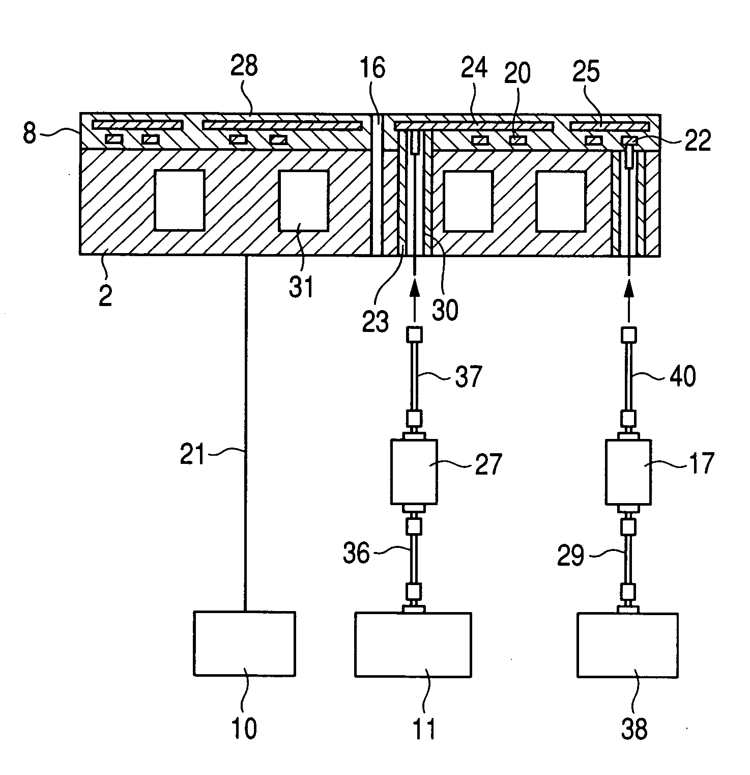
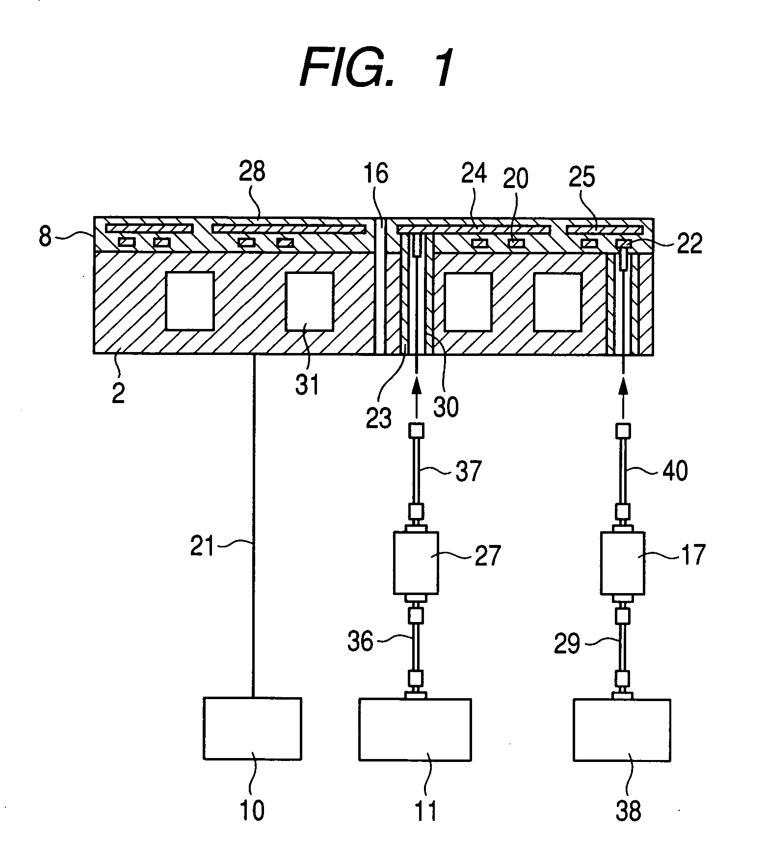
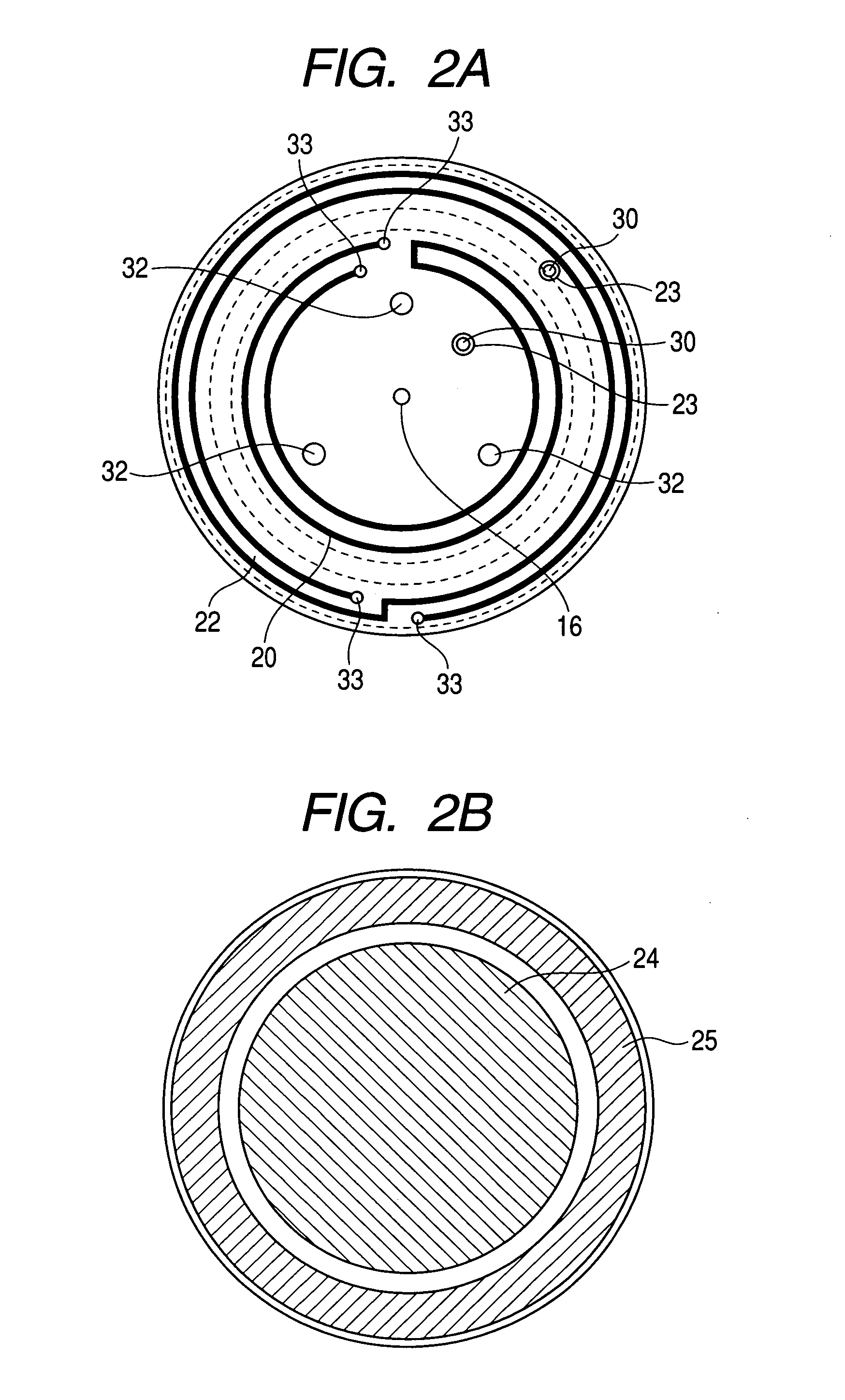
[0052]An electron-cyclotron-resonance (ECR) plasma processing apparatus according to a first embodiment of the present invention will be described with reference to FIGS. 1 to 5. FIG. 1 is a schematic sectional view of a so-called “bipolar electrostatic chuck” according to this embodiment. FIG. 2A is a drawing showing an example of a heat pattern according to this embodiment. FIG. 2B is a drawing showing an example of an electrostatic chuck pattern according to this embodiment. FIG. 3 is a schematic sectional view of the effective magnetic field microwave plasma processing apparatus according to this embodiment.

[0053]In the plasma processing apparatus including the bipolar electrostatic chuck according to the first embodiment, two heaters having approximately identical areas are disposed below two chuck electrodes having approximately identical areas so that they are completely hidden behind the corresponding chuck electrodes. Thus, a potential difference is prevented from being mad...

second embodiment

[0081]In the first embodiment, the two heaters having approximately identical areas are disposed below the two chuck electrodes having approximately identical areas so that the heaters are completely hidden behind the chuck electrodes.

[0082]However, the number of heaters for controlling the wafer temperature is not limited to two. According to the technical idea of the present invention, even if one heater is buried around the periphery (or inner circumference) of the electrostatic chuck, for example, in order to fine-tune the temperature of a wafer only around the periphery thereof, no damage occurs. In this case, it is sufficient to dispose a dummy-heater that has an area approximately identical to that of the outer heater disposed around the periphery and is not coupled to the heater power supply, in a layer lower the inner electrostatic chuck electrode, and to couple a coaxial cable having a length L approximately identical to that of a cable coupled to the outer heater, to this...

third embodiment

[0083]FIG. 6 shows a third embodiment of the present invention. In this embodiment, the inner heater according to the first embodiment includes a ground circuit for coupling a variable capacitor 51 to a ground via the inner heater, in addition to the circuit including the coaxial cable and filter coupled to the heater power supply. By adjusting the capacitance of the variable capacitor 51, the capacitance from the inner heater to a ground is made identical to that from the outer heater to a ground. Thus, the high-frequency voltage on the inner electrostatic chuck electrode and that on the outer electrostatic chuck electrode are made approximately identical. As a result, the potential difference on the wafer is made approximately zero. This is an effective solution in a case where the inner and outer heaters have different areas and thus the capacitances C41 and C42 are different.

[0084]According to this embodiment, the potential difference on a wafer made in a case where plasma is di...


PUM

PropertyMeasurementUnit
lengthaaaaaaaaaa
lengthaaaaaaaaaa
frequencyaaaaaaaaaa

Abstract

A plasma processing apparatus is provided that includes a heater-built-in electrostatic chuck, prevents a direct-current potential difference from being made in the plane of a wafer during plasma processing, and performs plasma processing while controlling the temperature of the wafer with good responsiveness without damaging a semiconductor device. The heater-built-in electrostatic chuck of the plasma processing apparatus has a structure in which an insulator, two heaters, an insulator, two electrostatic chuck electrodes having approximately identical areas, and a dielectric film are laminated in ascending order on a conductive base material to which a bias voltage is to be applied. The heaters have approximately identical areas, and are disposed below the two electrostatic chuck electrodes, respectively. Power is provided to the heaters via a low-path filter and a coaxial cable.

Description

CLAIM OF PRIORITY[0001]The present application claims priority from Japanese application JP 2008-4414 filed on Jan. 11, 2008, the content of which is hereby incorporated by reference into this application.FIELD OF THE INVENTION[0002]The present invention relates to a plasma processing apparatus for processing a semiconductor wafer. In particular, the invention relates to a plasma processing apparatus that processes a semiconductor wafer while holding it with a heater-built-in electrostatic chuck.BACKGROUND OF THE INVENTION[0003]Circuit patterns to be processed into semiconductor wafers have increasingly been made finer as the packing density of semiconductor elements is increased. Accordingly, more stringent processing dimensional accuracies have been required. Under these circumstances, it is extremely important to temperature-control a wafer (semiconductor wafer) being processed.[0004]For example, if a wafer is etched using plasma, a high-frequency voltage is normally applied to t...

Claims


Application Information

Patent Timeline
Patent Type & Authority Applications(United States)
IPC IPC(8): H01L21/3065
CPCH01L21/6831H01L21/67103
Inventor KANNO, SEIICHIROTSUBONE, TSUNEHIKOKITADA, HIROHO
Owner HITACHI HIGH-TECH CORP
Learn More