Printed circuit board and semiconductor package including the same

a technology of printed circuit board and semiconductor package, which is applied in the association of printed circuit non-printed electric components, electrical apparatus construction details, and second resist masks. it can solve the problems of deteriorating affecting the reliability and increasing the thickness of a semiconductor package. it can prevent the delamination of a sealant, and achieve the effect of preventing voids

Inactive Publication Date: 2009-07-16
SAMSUNG ELECTRONICS CO LTD
View PDF1 Cites 9 Cited by
  • Summary
  • Abstract
  • Description
  • Claims
  • Application Information

AI Technical Summary

Benefits of technology

[0008]Embodiments of the present invention provide a printed circuit board (PCB) that is configured to prevent voids and delamination of a sealant.

Problems solved by technology

However, when adhesives, such as epoxy, are used to attach a semiconductor chip to a semiconductor package substrate, an increase in the thickness of the semiconductor package may result, as well as the introduction of various other problems.
However, as the thickness of a semiconductor chip is reduced, fine voids are generated, thereby deteriorating the reliability of a semiconductor package.
In addition, delamination may occur between a semiconductor package substrate and a sealant, thereby deteriorating the reliability of a semiconductor package and increasing the failure rate of semiconductor packages.

Method used


Image

  • Printed circuit board and semiconductor package including the same
  • Printed circuit board and semiconductor package including the same
  • Printed circuit board and semiconductor package including the same

Examples


Embodiment Construction

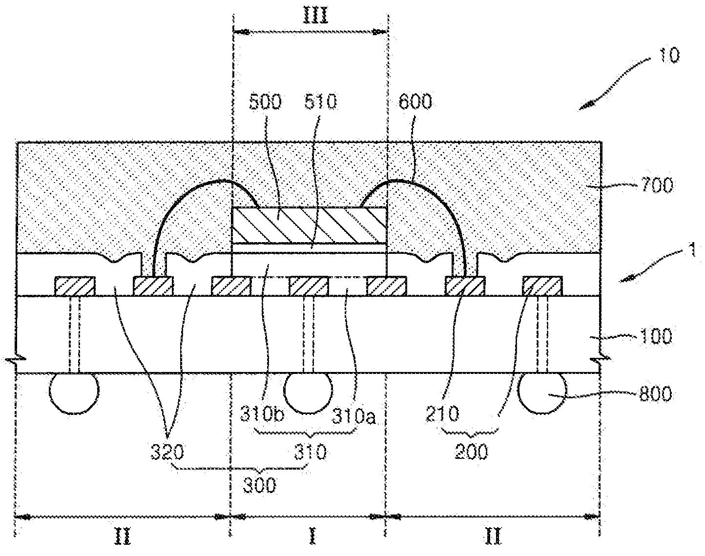
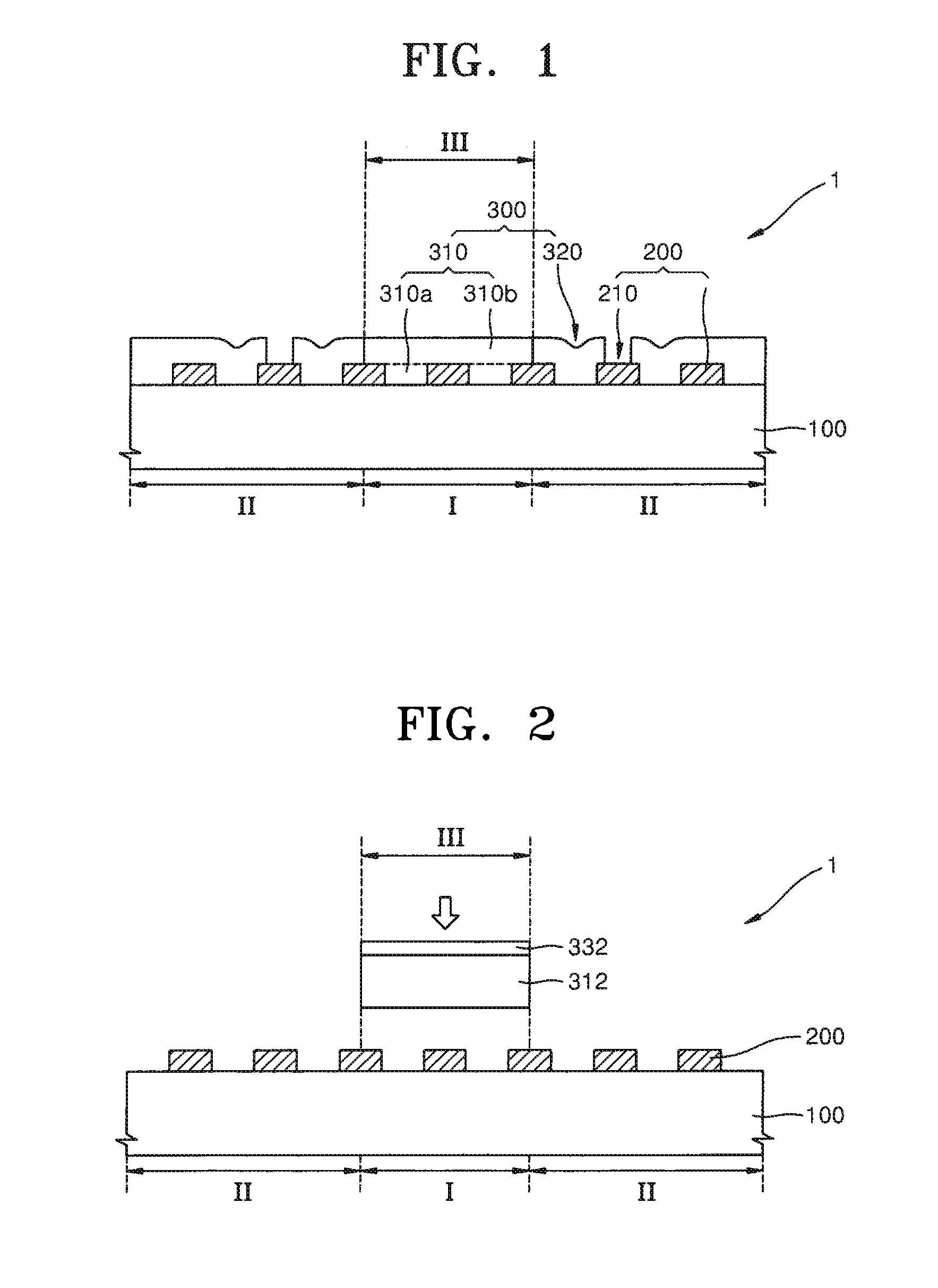
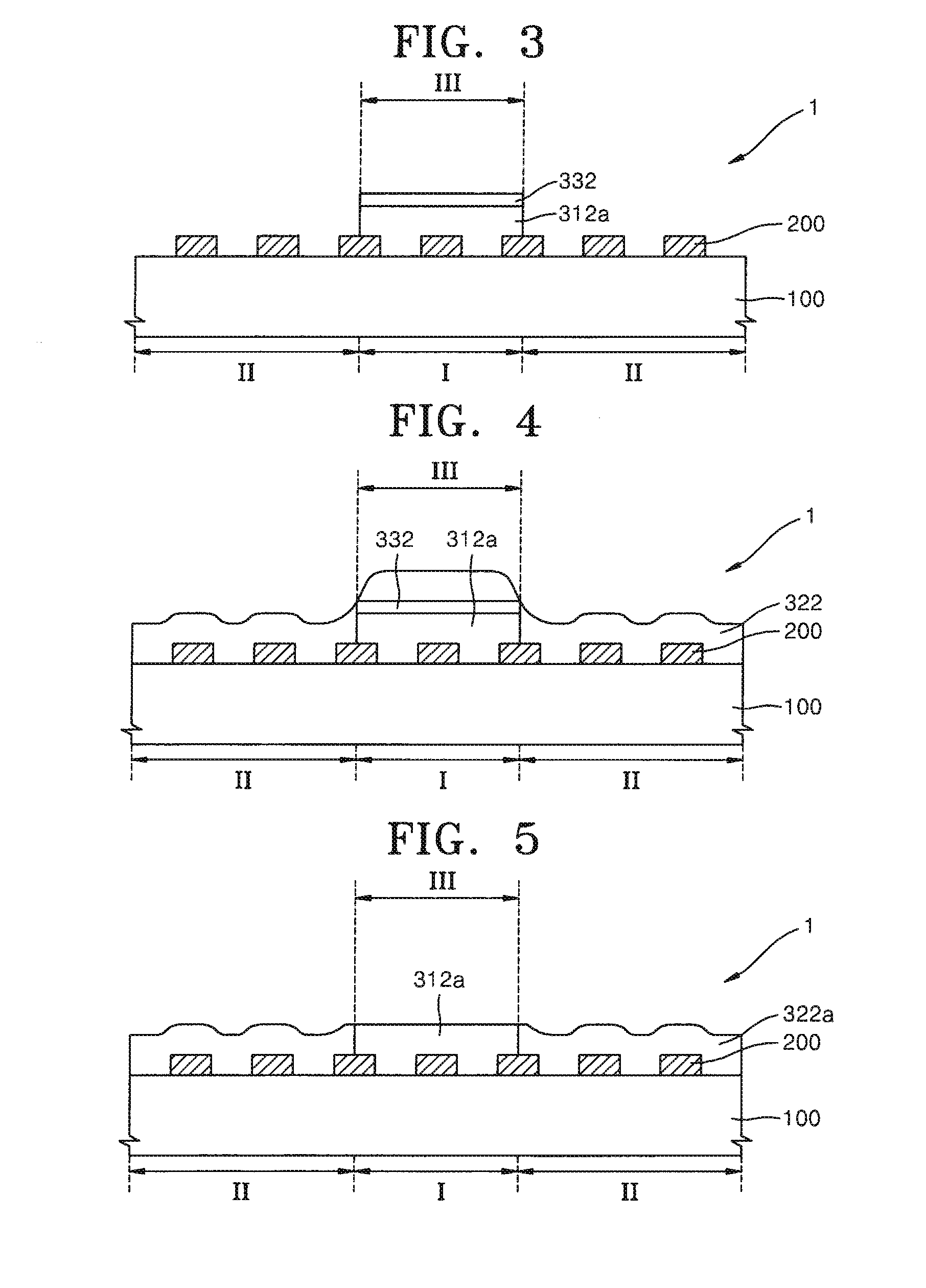
[0025]The present invention will now be described more fully with reference to the accompanying drawings, in which exemplary embodiments of the invention are shown. The invention may, however, be embodied in many different forms and should not be construed as being limited to the embodiments set forth herein; rather, these embodiments are provided so that this disclosure will be thorough and complete, and will fully convey the concept of the invention to one of ordinary skill in the art. It will also be understood that when a layer is referred to as being “on” another layer or substrate, it can be directly on the other layer or substrate, or intervening layers may also be present. In the drawings, the thicknesses of layers and regions are exaggerated for clarity. The same reference numerals in the drawings denote the same element. The terms are only for illustrative purposes and are not intended to limit the scope of the present invention.

[0026]FIG. 1 is a cross-sectional view of a ...


PUM

PropertyMeasurementUnit
surface roughnessaaaaaaaaaa
conductiveaaaaaaaaaa

Abstract

A printed circuit board (PCB) and a semiconductor package that are configured to prevent delamination and voids. In one example embodiment, the semiconductor package includes a PCB having a base substrate on which conductive patterns are formed and which includes an interior region having a die paddle for receiving a semiconductor chip and an exterior region disposed outside the interior region. The PCB also includes a first solder resist formed on a portion of the base substrate corresponding to the interior region and a second solder resist formed on a portion of the base substrate corresponding to the exterior region. The second solder resist may also have a greater surface roughness than the surface roughness of the first solder resist.

Description

CROSS-REFERENCE TO RELATED PATENT APPLICATION[0001]This application claims the benefit of Korean Patent Application No. 10-2008-0004427, filed on Jan. 15, 2008, in the Korean Intellectual Property Office, the disclosure of which is incorporated herein by reference.BACKGROUND[0002]1. Field of the Invention[0003]The present invention relates to a printed circuit board (PCB) used for manufacturing a semiconductor package and a semiconductor package including the PCB, and more particularly, to a PCB to which a semiconductor chip is attached using an adhesive tape and a semiconductor package including the PCB.[0004]2. Description of the Related Art[0005]To meet the demands of consumers for smaller and lighter electronic devices, a need to further miniaturize and reduce the size and weight of semiconductor devices within these electronic devices is apparent. In addition, it is also desirable for these semiconductor devices to have similar or improved performance characteristics over previ...

Claims


Application Information

Patent Timeline
Patent Type & Authority Applications(United States)
IPC IPC(8): H01L23/485H05K1/18
CPCH05K3/3452Y10T29/4913H05K2201/09881H05K2203/0191H05K2203/049H05K2203/0577H05K2203/058H05K2203/0582H05K2203/0585H05K2203/1476H01L2224/16145H01L2224/32145H01L2224/32225H01L2224/48091H01L2224/48227H01L2224/73265H01L2924/15311H05K2201/09772H01L2225/06562H01L2924/00012H01L2924/00014H01L2924/00H01L24/73H05K1/09
Inventor OH, YUN-JINHAN, CHANG-HOONLEE, KWANG-RYULKIM, HYOUNG-SUK
Owner SAMSUNG ELECTRONICS CO LTD
Why Eureka
Try Eureka