

Display device and method of manufacturing transparent substrate for display device
a technology of display device and transparent substrate, which is applied in the direction of identification means, instruments, non-linear optics, etc., can solve the problems of loss of light, difficult to effectively retrieve or pick up the light generated in the display device or that has been introduced into the display device, and reflection and glar
- Summary
- Abstract
- Description
- Claims
- Application Information
AI Technical Summary
Benefits of technology
Problems solved by technology
Method used
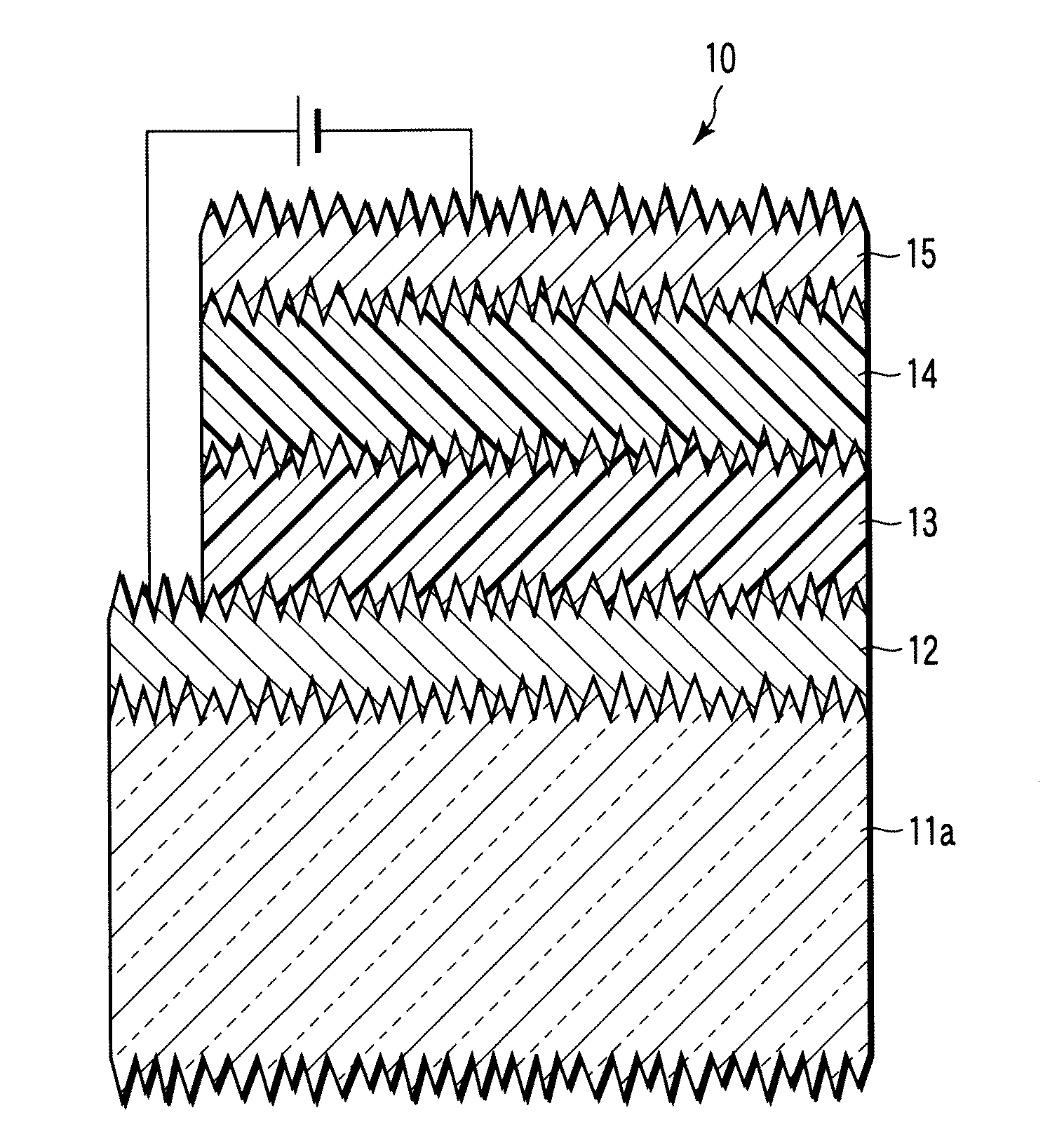
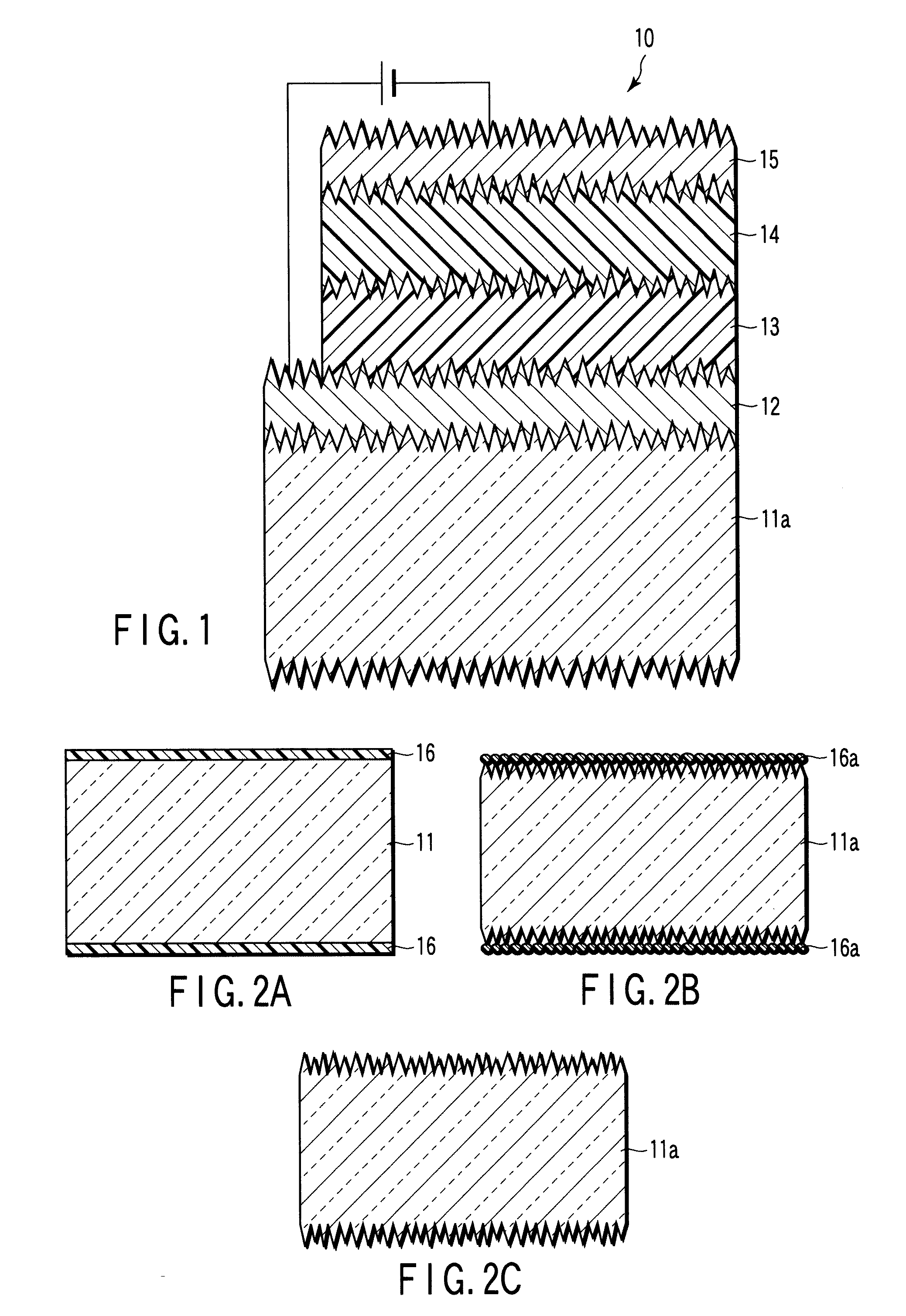
Image

Examples
example 1
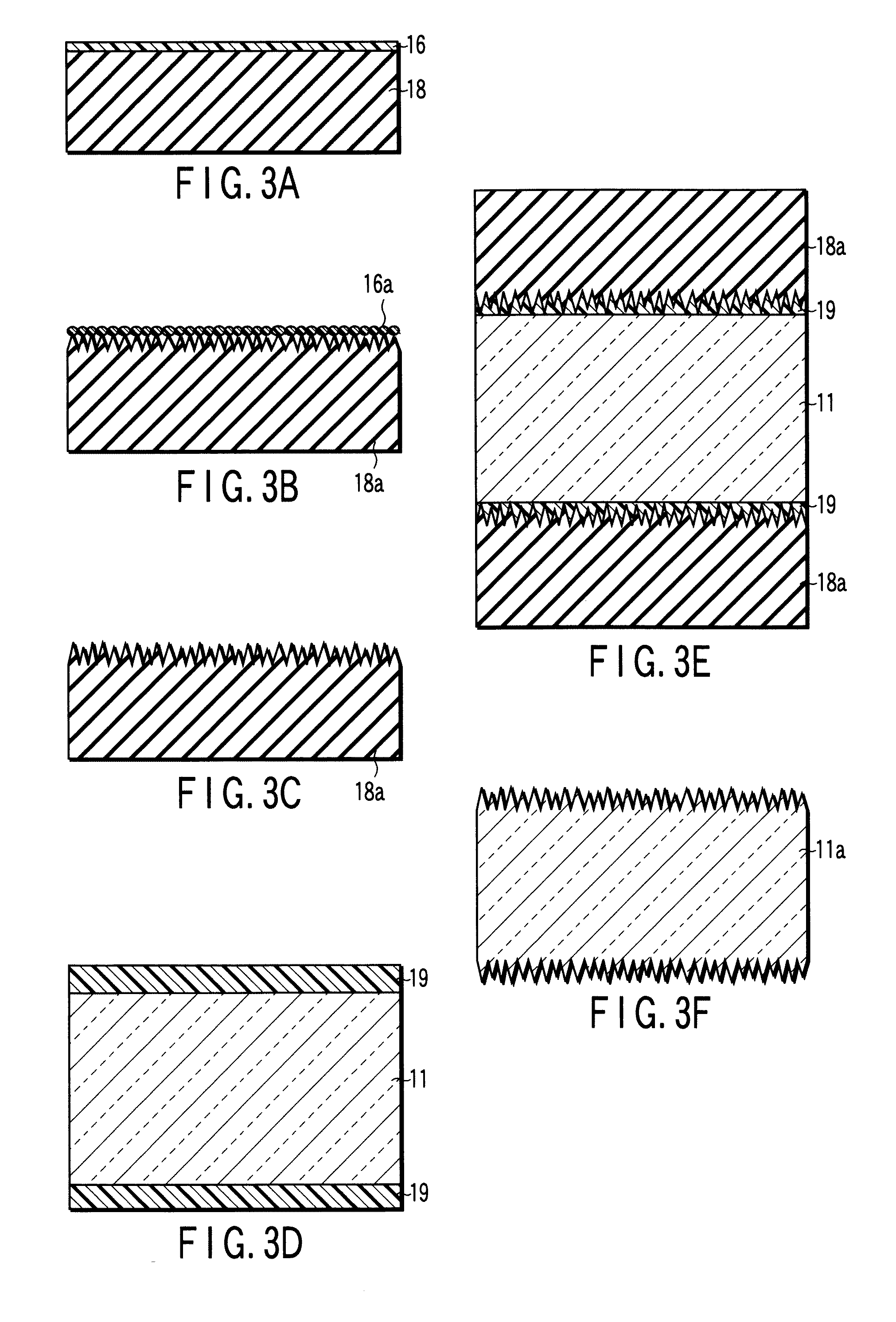
[0147]First of all, a block copolymer comprising polystyrene (PS) and methyl polymethacrylate (PMMA) was dissolved in propylene glycol monomethyl ether acetate (PGMEA) used as a solvent to prepare a solution of polymer. The molecular weight of the PS included in the block copolymer was 154800 and the molecular weight of the PMMA included therein was 392300, Mw / Mn of the block copolymer being 1.08.
[0148]This solution of polymer was then coated on the surface of a flat glass substrate by spin coating method at a rotational speed of 2500 rpm to form a coated film. This coated film was then prebaked at a temperature of 110° C. for 90 seconds to vaporize the solvent, thus forming a polymer layer having a thickness of 100 nm.
[0149]Then, the polymer layer was annealed at a temperature of 210° C. for 4 hours in a nitrogen gas atmosphere to phase-separate the PS from the PMMA in the block copolymer. Further, under the conditions of: 30 sccm in flow rate of CF4, 1.33 Pa (10 mTorr) in pressure...
example 2
[0155]In the same manner as described in Example 1, a polymer film comprising a PS-PMMA block copolymer was formed on a flat glass substrate and annealed to annealing to phase-separate the PS from the PMMA. Then, PS and PMMA were subjected to etching by RIE under the conditions of: 30 sccm in flow rate Of O2, 13.3 Pa (100 mTorr) in pressure and 100 W in electric power. In contrast to the case where CF4 was used as an etching gas, the use of O2 gas as an etching gas was ineffective in etching the substrate. However, due to the use of O2 gas, the PMMA was selectively etched, thus enabling the formation of a mask layer consisting of a pattern of the PS.
[0156]By using this mask layer, the surface of the glass substrate was dry-etched by RIE in the same manner as described in Example 1. As a result, it was possible to form fine recessed / projected portions on the surface of the glass substrate, wherein the projected portions thereof were featured in that the diameter thereof was about 70 ...
example 3
[0159]First of all, by using a block copolymer comprising PS and PMMA was dissolved in PGMEA used as a solvent to prepare a solution of polymer. The molecular weight of the PS included in the block copolymer was 315000 and the molecular weight of the PMMA included therein was 785000, Mw / Mn of the block copolymer being 1.08.
[0160]This solution of polymer was then coated on the surface of a flat glass substrate by spin coating method at a rotational speed of 3000 rpm to form a coated film. This coated film was then prebaked at a temperature of 110° C. for 90 seconds to vaporize the solvent, thus forming a polymer layer having a thickness of 150 nm.
[0161]Then, the polymer layer was annealed at a temperature of 210° C. for 4 hours in a nitrogen gas atmosphere to phase-separate the PS from the PMMA in the block copolymer. Further, under the conditions of: 30 sccm in flow rate Of O2, 13.3 Pa (100 mTorr) in pressure and 100 W in electric power, the polymer layer was dry-etched by RIE. Due ...
PUM
| Property | Measurement | Unit |
|---|---|---|
| diameter | aaaaa | aaaaa |
| diameter | aaaaa | aaaaa |
| reflectance | aaaaa | aaaaa |
Abstract
Description
Claims
Application Information