Semiconductor memory device and method of controlling the same

a memory device and memory technology, applied in the direction of instruments, coding, code conversion, etc., can solve the problems of data loss, information retained in the memory cell can be lost along with the elapse of time, and errors can rarely occur in the information field,

Active Publication Date: 2009-07-16
KIOXIA CORP
View PDF7 Cites 94 Cited by
  • Summary
  • Abstract
  • Description
  • Claims
  • Application Information

AI Technical Summary

Problems solved by technology

If the elapsed time has reached a predetermined length, the data may be lost.
For this reason, the information retained in the memory cell can be lost along with the elapse of time (an error can occur in the information).
If the elapsed time from the information storage time is short, an error can rarely occur in the information.
On the other hand, if a long time has elapsed after information storage, an error may occur in the inf

Method used


Image

  • Semiconductor memory device and method of controlling the same
  • Semiconductor memory device and method of controlling the same
  • Semiconductor memory device and method of controlling the same

Examples


Embodiment Construction

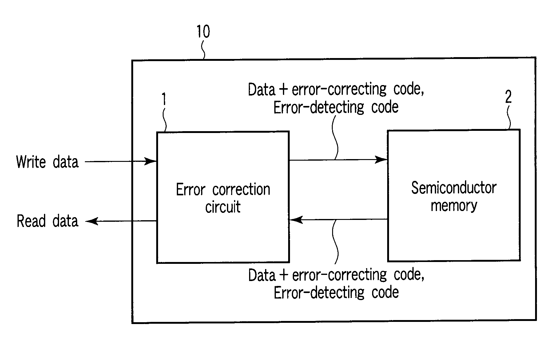
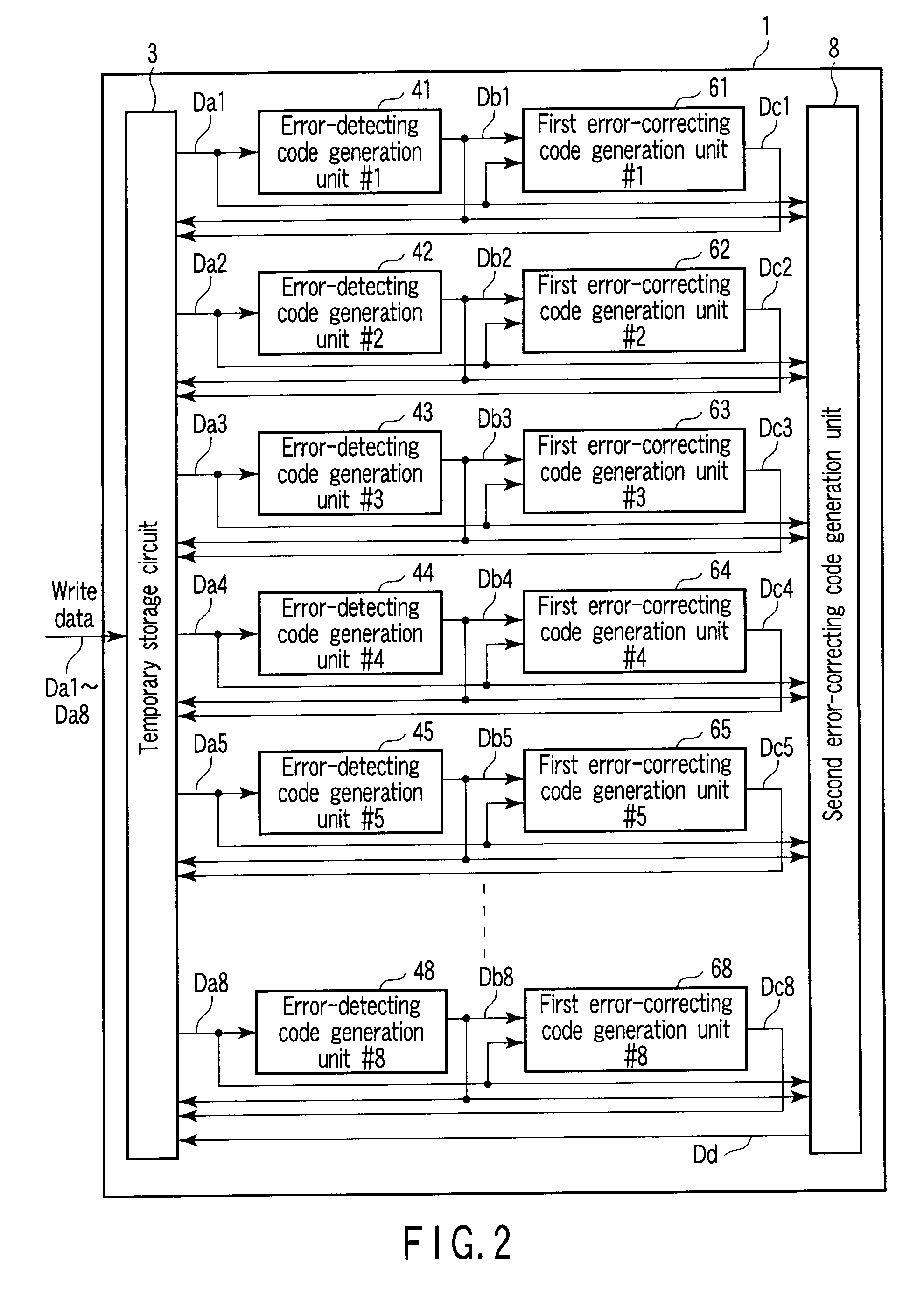
[0028]An embodiment of the present invention will now be described with reference to the accompanying drawing. In the following description, the same reference numerals denote constituent elements having almost the same functions and arrangements, and a repetitive explanation will be made only when necessary.

[0029]The embodiments to be described below are mere examples of an apparatus or method to embody the technical scope of the present invention. The technical scope of the present invention does not limit the materials, shapes, structures, and arrangements of the components to those described below. The technical scope of the present invention allows various changes and modifications in the appended claims.

[0030]The functional blocks of the embodiments of the present invention can be implemented by hardware, computer software, or a combination thereof. The blocks will be described below generally from the viewpoint of their functions while clarifying that they can be implemented ...


PUM


Abstract

A semiconductor memory device includes a plurality of detecting code generators configured to generate a plurality of detecting codes to detect errors in a plurality of data items, respectively, a plurality of first correcting code generators configured to generate a plurality of first correcting codes to correct errors in a plurality of first data blocks, respectively, each of the first data blocks containing one of the data items and a corresponding detecting code, a second correcting code generators configured to generate a second correcting code to correct errors in a second data block, the second data block containing the first data blocks, and a semiconductor memory configured to nonvolatilely store the second data block, the first correcting codes, and the second correcting code.

Description

CROSS-REFERENCE TO RELATED APPLICATIONS[0001]This is a Continuation Application of PCT Application No. PCT / JP2008 / 063344, filed Jul. 17, 2008, which was published under PCT Article 21(2) in Japanese.[0002]This application is based upon and claims the benefit of priority from prior Japanese Patent Application No. 2007-225996, filed Aug. 31, 2007, the entire contents of which are incorporated herein by reference.BACKGROUND OF THE INVENTION[0003]1. Field of the Invention[0004]The present invention relates to a semiconductor memory device and a method of controlling the same and, for example, to a memory device which nonvolatilely stores information and has an error correction circuit, and a method of controlling the memory device.[0005]2. Description of the Related Art[0006]In some kinds of nonvolatile memory devices, the state of the physical quantity that controls data storage changes along with the elapse of time. If the elapsed time has reached a predetermined length, the data may ...

Claims


Application Information

Patent Timeline
IPC IPC(8): H03M13/05G06F11/22G06F11/07
CPCG06F11/1068G06F11/1008H03M13/03G06F11/10H03M13/2906H03M13/29G06F13/1673G06F13/4068Y02D10/00G06F11/1012H03M13/35G11C29/52G06F11/1004H03M13/6561
Inventor KANNO, SHINICHIUCHIKAWA, HIRONORI
Owner KIOXIA CORP
Why Eureka
Try Eureka