Wiring board and method of manufacturing the same

a wiring board and manufacturing method technology, applied in the direction of superimposed coating process, resistive material coating, liquid/solution decomposition chemical coating, etc., can solve the problem of enlargement of the area of the alloy layer bm, entanglement of the wiring board, and the flip chip bonding type of conventional electronic components. problems, to achieve the effect of reducing cost and eliminating warps

Active Publication Date: 2009-07-23
SHINKO ELECTRIC IND CO LTD
View PDF2 Cites 16 Cited by
  • Summary
  • Abstract
  • Description
  • Claims
  • Application Information

AI Technical Summary

Benefits of technology

[0014]An object of the present invention is to provide a wiring board and a method of manufacturing the same, which are capable of, even if a stress is generated between the wiring board and an electronic component to be mounted due to a difference in the coefficient of thermal expansion therebetween, effectively absorbing the stress and thereby ensuring that electrical connection between the wiring board and the electronic component is maintained, and are also capable of substantially eliminating a warp in the wiring board after mounting and thereby contributing to a reduction in cost.

Problems solved by technology

However, the conventional electronic component device of the flip chip bonding type encounters problems as given below when subjected to such a test for reliability evaluation.
Also, the alloy layer BM has another problem.
When a high-temperature exposure test (e.g., a test in which device test target is left in an environment at a temperature of 150° C. for a given period of time) is performed, heat facilitates the flowing of atoms of metal, thus causing an enlargement of the area of the alloy layer BM, and in turn, an increase in the likelihood of occurrence of break-off.
However, “break-off” in such a conductive bump can possibly occur likewise even in the case of bonding using the same metal.
However, the following problems arise.
The method requires a process for filling the underfill resin 70 into the gap between the wiring board 50 and the chip 60, and hence causes a problem of an increase in man-hours and a rise in cost.
Further, delamination of the chip 60 may possibly occur depending on the degree of warp, thus causing deterioration in the reliability of connection.

Method used


Image

  • Wiring board and method of manufacturing the same
  • Wiring board and method of manufacturing the same
  • Wiring board and method of manufacturing the same

Examples


first embodiment

. . . see FIG. 1 to FIGS. 5A to 5D

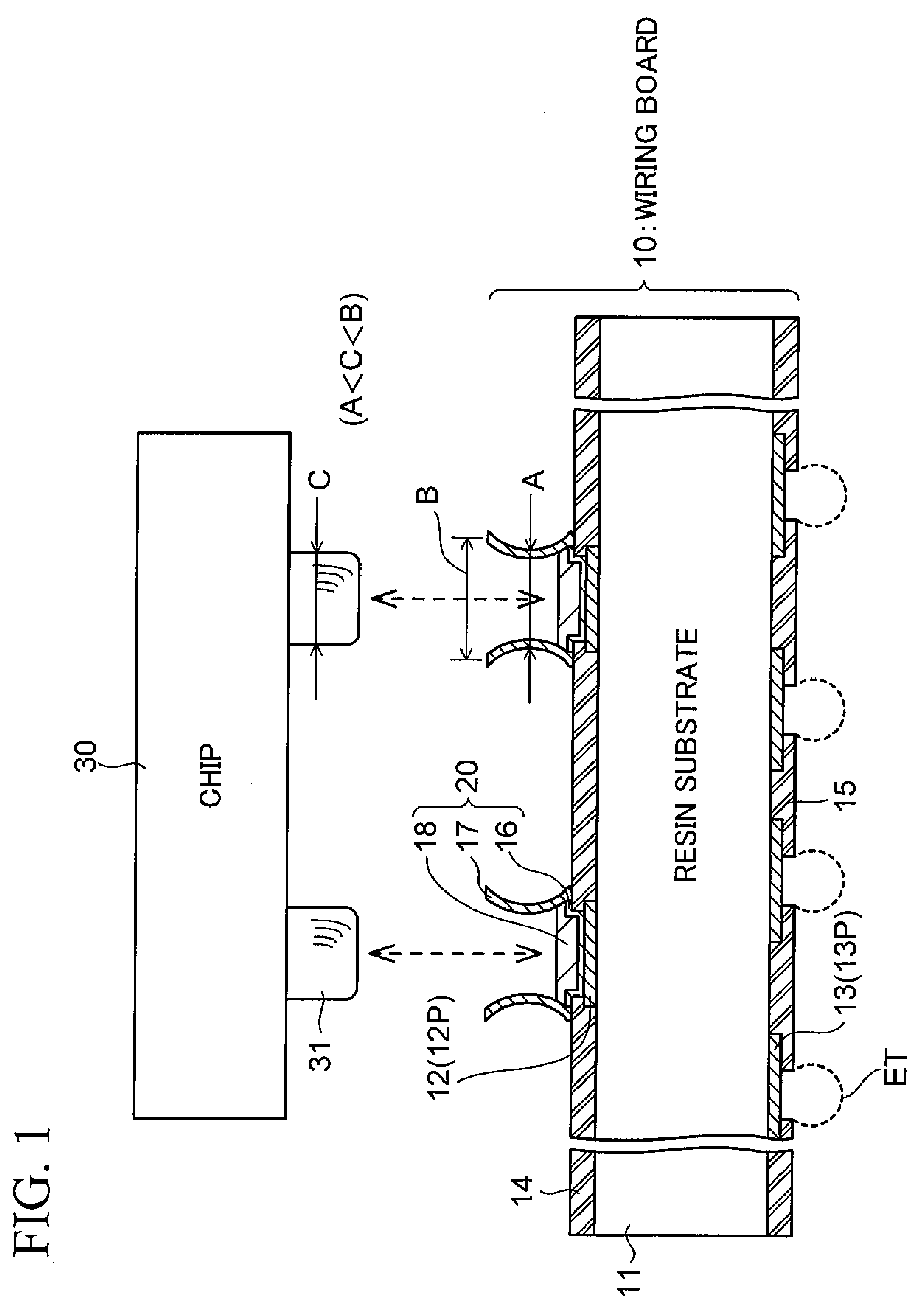
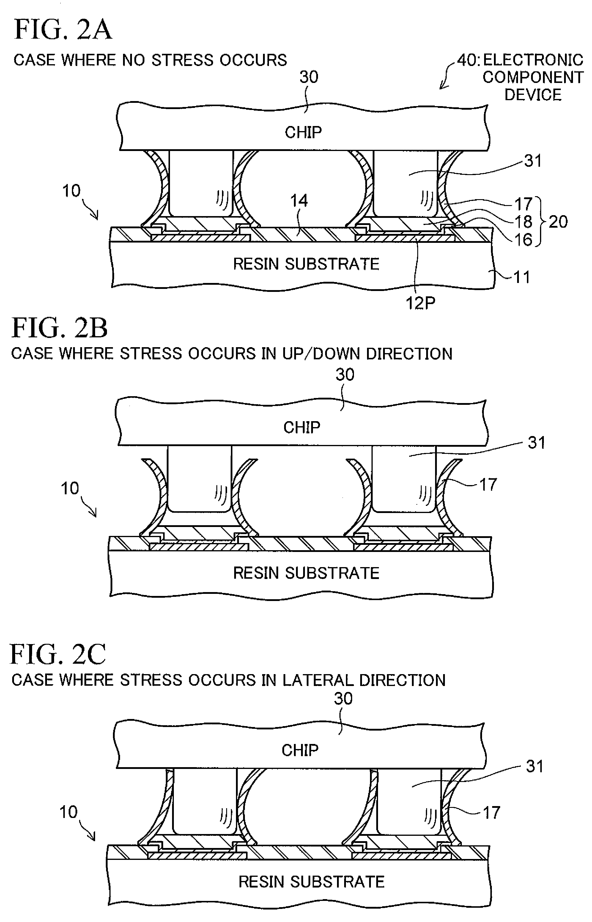
[0031]FIG. 1 shows in a sectional form the configuration of a wiring board according to a first embodiment of the present invention. As shown in FIG. 1, a wiring board 10 according to the embodiment is illustrated as being capable of detachably mounting a semiconductor chip 30 to function as an electronic component.

[0032]The wiring board 10 of this embodiment is basically configured by including a resin substrate 11 which forms a wiring board body; wiring layers 12 and 13 formed by patterning in desired layouts on both surfaces, respectively, of the resin substrate 11; and insulating layers 14 and 15 to function as protection films, formed to cover both surfaces exclusive of pad portions 12P and 13P defined in desired positions of the wiring layers 12 and 13, respectively. Further, the wiring board 10 is provided with external connection terminals 20 characterizing the present invention, in desired positions on the insulating layer (the upper insula...

second embodiment

. . . see FIGS. 8A to 8B

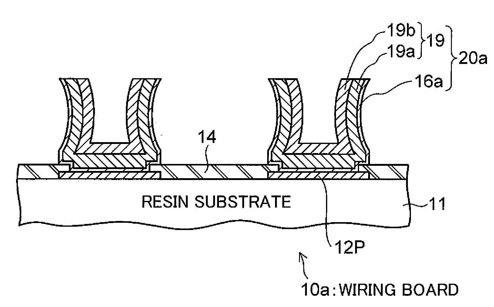
[0064]A wiring board 10a according to a second embodiment (see FIG. 7C) has basically the same configuration as the wiring board 10 according to the first embodiment (FIG. 1), but is different in that the wiring board 10a is provided with a cylindrically-shaped terminal (an external connection terminal) 20a having a different configuration from the first embodiment in a desired position on the insulating layer 14 on the chip mounting surface side. As shown in FIG. 7C, the cylindrically-shaped terminal 20a consists of a conductor layer (a base portion) 16a whose portion (bottom) is electrically connected to the pad portion 12P exposed from the insulating layer 14 and which is curvedly formed in the shape of a cylinder; and a conductor layer (a cylindrically-shaped conductor portion) 19 of two-layer structure coating the overall inner surface of the cylindrically-shaped base portion 16a.

[0065]The shapes of the cylindrically-shaped conductor portion 19, as view...


PUM

PropertyMeasurementUnit
temperatureaaaaaaaaaa

Abstract

A wiring board includes an external connection terminal of a cylindrical shape, in which an electrode terminal of the electronic component to be mounted is fitted. In one configuration, a portion of the external connection terminal is electrically connected to a pad portion formed on an electronic component mounting surface side of the wiring board, and the external connection terminal is curvedly formed in such a shape that the outer periphery of the electrode terminal comes into close contact with the inner periphery of the middle portion of the external connection terminal when the electrode terminal is inserted into the external connection terminal.

Description

CROSS-REFERENCE TO RELATED APPLICATIONS[0001]This application is based on and claims priority of Japanese Patent Application No. 2008-010489 filed on Jan. 21, 2008, the entire contents of which are incorporated herein by reference.BACKGROUND OF THE INVENTION[0002](a) Field of the Invention[0003]The present invention relates to a technique of mounting an electronic component such as a semiconductor device on a wiring board, and more particularly to a wiring board (hereinafter also referred to as “package” for the sake of convenience) adapted to detachably mount an electronic component thereon, and to a method of manufacturing the same.[0004](b) Description of the Related Art[0005]For surface mounting of an electronic component (a chip) such as a semiconductor device on a wiring board (a package), wire bonding, flip chip bonding or the like is used as means for providing an electrical connection between the chip and the package. The wire bonding requires a bonding area (an area having...

Claims


Application Information

Patent Timeline
Patent Type & Authority Applications(United States)
IPC IPC(8): H05K1/11B05D5/12
CPCH05K3/062H05K3/326H01L2924/01322H01L2224/73204H01L2224/32225H01L2224/16225H05K2201/10674H05K3/4007H05K3/4092H05K2201/0311H05K2201/0338H05K2201/068H05K2201/1059H01L2924/00H01L2224/81141H01L2224/05567H01L2224/05573H01L2224/05624H01L2224/13011H01L2224/81193H01L2924/00014
Inventor SUNOHARA, MASAHIROMURAYAMA, KEIYAMANO, TAKAHARU
Owner SHINKO ELECTRIC IND CO LTD
Why Eureka
Try Eureka