Plasma display device

Inactive Publication Date: 2009-07-23
PANASONIC CORP
View PDF8 Cites 2 Cited by
  • Summary
  • Abstract
  • Description
  • Claims
  • Application Information

AI Technical Summary

Benefits of technology

[0010]With this structure, even when an image signal increasing the power consumption of the data electrode driver circuit is supplied, the plasma display device is capable of promptly responding to a rapid increase in the power consumption or the like, and making a stable operation to display images without causing malfunction of the data electrode driver circuit.
[0017]With this structure, even without changing the coding table, only stopping the address operation in a corresponding subfield can reduce the power consumption of the data electrode driver circuit.

Problems solved by technology

The power consumption of the data electrode driver circuit is not only due to the discharge caused by the address discharge.
Rather, the power consumption caused by charging and discharging the capacitance of these data electrodes constitutes a larger proportion.
However, when the address pulse voltage is applied to the data electrodes at random, the charge / discharge current and thus the power consumption are large.
However, as the size and definition of the panel is increasing, the maximum power consumption becomes far larger than the power consumed when a normal image is displayed.
It is uneconomical to design the power supply for data electrodes so that necessary power can be supplied even in such a case.
In this method, the power consumption of the data electrode driver circuit is actually detected, and the gradations are limited at large power consumption.
However, in the methods of limiting gradations according to the power consumption in the data electrode driver circuit, as disclosed in Patent Document 1 and Patent Document 2, for example, a phenomenon of repeating increases and decreases in power consumption in a short cycle is more likely to occur.
This operation can hinder stable display operation by pausing image display for protection or the like.
On the other hand, in the method of limiting gradations according to the temperature in the data electrode driver circuit as disclosed in Patent Document 3, frequent protecting operation of the protective circuit can be inhibited; however, a prompt response to a rapid increase in power consumption or the like cannot be made.
Further, repeated increases and decreases in power consumption and temperature cause repetition between limitation and non limitation of gradations.
This repetition between gradation limitation and non limitation causes flickers in the display image, thus degrading the image.

Method used


Image

  • Plasma display device
  • Plasma display device
  • Plasma display device

Examples


first exemplary embodiment

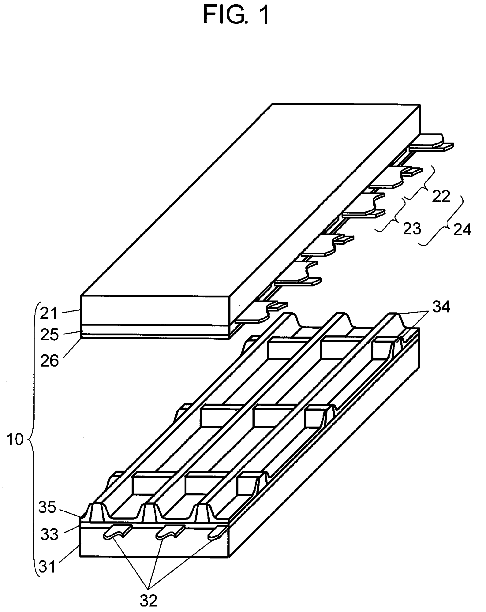
[0071]FIG. 1 is an exploded perspective view illustrating an essential part of panel 10 in accordance with the first exemplary embodiment of the present invention. In panel 10, front substrate 21 and rear substrate 31 both made of a glass are faced to each other so that a discharge space is formed therebetween. A plurality of scan electrodes 22 and sustain electrodes 23 constituting display electrode pairs 24 are formed on front substrate 21 in parallel with each other. Dielectric layer 25 is formed to cover scan electrodes 22 and sustain electrodes 23. Protective layer 26 is formed over dielectric layer 25. A plurality of data electrodes 32 are formed on rear substrate 31. Dielectric layer 33 is formed to cover data electrodes 32. On dielectric layer 33, barrier ribs 34 are provided in a double cross shape. Further, over the surface of dielectric layer 33 and side faces of barrier ribs 34, phosphor layers 35 are provided. Front substrate 21 and rear substrate 31 are faced to each o...

second exemplary embodiment

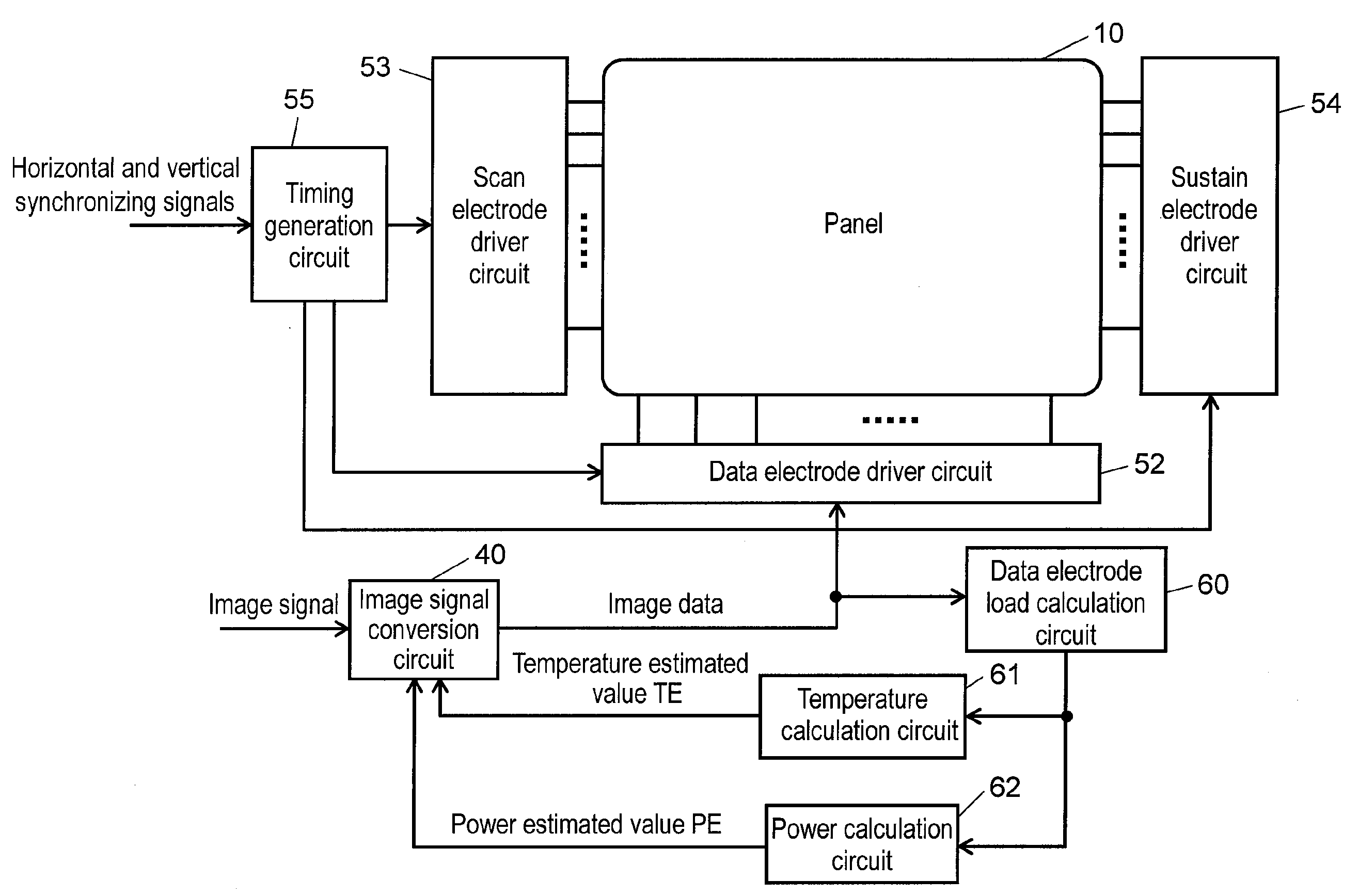
[0131]FIG. 8 is a circuit block diagram of a plasma display device in accordance with the second exemplary embodiment of the present invention. The plasma display device of this exemplary embodiment includes the following elements: panel 10; image signal conversion circuit 400; data electrode driver circuit 52; scan electrode driver circuit 53; sustain electrode driver circuit 54; timing generation circuit 55; data electrode load calculation circuit 60; temperature calculation circuit 61 as a temperature calculator; power calculation circuit 62 as a power calculator; temperature change detection circuit 63 as a temperature change detector; power change detection circuit 64 as a power change detector; and a power supply (not shown) for supplying power necessary for the respective circuit blocks. In FIG. 8, elements denoted with the same reference marks as those in FIG. 4 have the same functions as those in FIG. 4, and detailed descriptions of those elements are omitted.

[0132]With ref...


PUM


Abstract

A plasma display device includes the following elements: an image signal conversion circuit for converting an image signal into an image data; a data electrode driver circuit for driving data electrodes according to the image data; a power calculation circuit for calculating a power consumption of the data electrode driver circuit according to the image data; and a temperature calculation circuit for calculating a temperature of the data electrode driver circuit according to the image data. The image signal conversion circuit converts the image signal into an image data decreasing the power consumption of the data electrode driver circuit at least when the calculated power consumption exceeds a predetermined power threshold value, or when the calculated temperature exceeds a predetermined temperature threshold value.

Description

[0001]THIS APPLICATION IS A U.S. NATIONAL PHASE APPLICATION OF PCT INTERNATIONAL APPLICATION PCT / JP2008 / 050229.TECHNICAL FIELD[0002]The present invention relates to a plasma display device for use in a wall-mounted television or a large monitor.BACKGROUND ART[0003]In a plasma display panel (hereinafter abbreviated as “panel”) representative of an image display device having a large number of pixels arranged in a plane shape, a large number of discharge cells are formed as the pixels between the front plate and the rear plate faced to each other. For the front plate, a plurality of display electrode pairs, each made of a scan electrode and a sustain electrode, are formed on a front glass substrate in parallel with each other. A dielectric layer and a protective layer are formed to cover these display electrode pairs. For the rear plate, a plurality of parallel data electrodes are formed on a rear glass substrate and a dielectric layer is formed over the data electrodes to cover them....

Claims


Application Information

Patent Timeline
IPC IPC(8): G06F3/038G09G3/28G09G3/288
CPCG09G3/2022G09G3/288G09G2320/0247G09G2360/16G09G2320/041G09G2320/0626G09G2330/021G09G2320/0271G09G3/296
Inventor YAMASHITA, TAKERUSAWA, KAZUKIYAMAMOTO, HIROKO
Owner PANASONIC CORP
Why Eureka
Try Eureka