

Semiconductor device
- Summary
- Abstract
- Description
- Claims
- Application Information
AI Technical Summary
Benefits of technology
Problems solved by technology
Method used
Image

Examples
Embodiment Construction
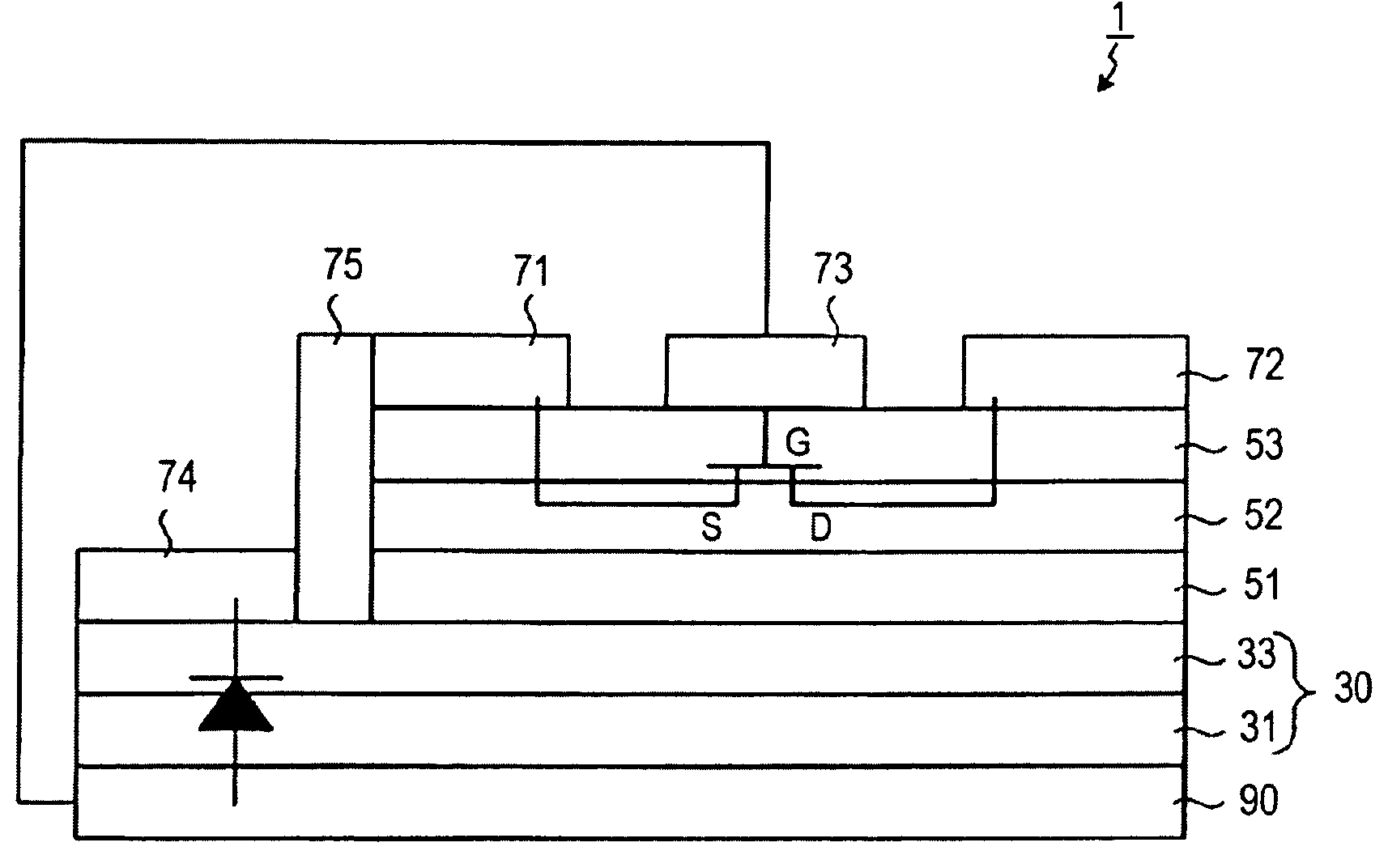
[0016]An exemplary embodiment of the semiconductor device of the present invention is explained below with reference to the accompanying drawings. The present invention is not limited by the embodiment. In the drawings, like reference numerals are used for like parts throughout the several views.
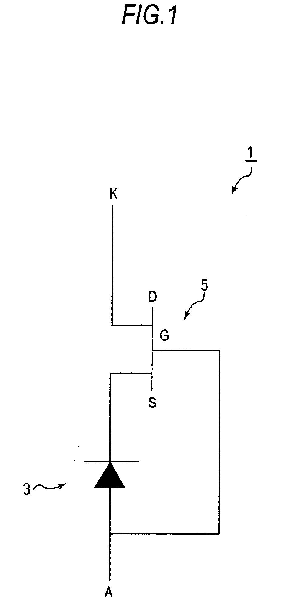
[0017]FIG. 1 is a circuit diagram showing a configuration of a semiconductor device 1 according to the present embodiment. As shown in FIG. 1, the semiconductor device 1 according to the embodiment includes a silicon diode 3 having a low breakdown voltage characteristic, and a GaN-based HEMT 5 formed of a GaN-based compound semiconductor, having a high breakdown voltage characteristic and capable of operating with low loss. A source electrode of the GaN-based HEMT 5 is connected to a cathode of the silicon diode 3, and a gate electrode of the GaN-based HEMT 5 is connected to an anode of the silicon diode 3.
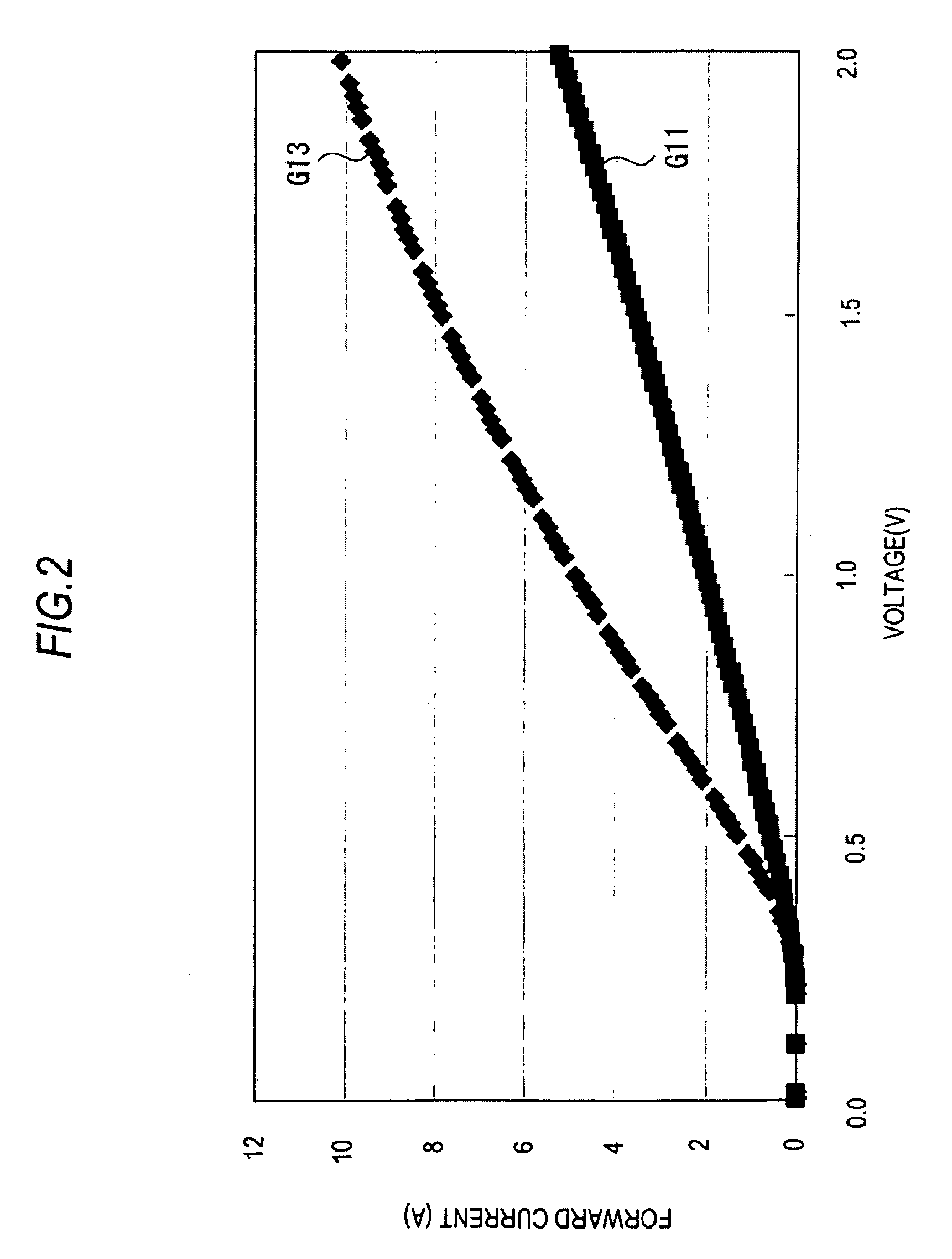
[0018]FIG. 2 is a graph showing a forward characteristic G11 of the semiconductor devi...
PUM
 Abstract
Description
Claims
Application Information