

Solid-state imaging device and method for manufacturing the same
a solid-state imaging and imaging device technology, applied in the direction of color television, television system, radio control device, etc., can solve the problem of insufficiently ensuring achieve high light blocking performance, enhance the ability of the light blocking above the black-level reference pixel, and reduce the thickness of the interconnect layer
- Summary
- Abstract
- Description
- Claims
- Application Information
AI Technical Summary
Benefits of technology
Problems solved by technology
Method used
Image

Examples
second embodiment
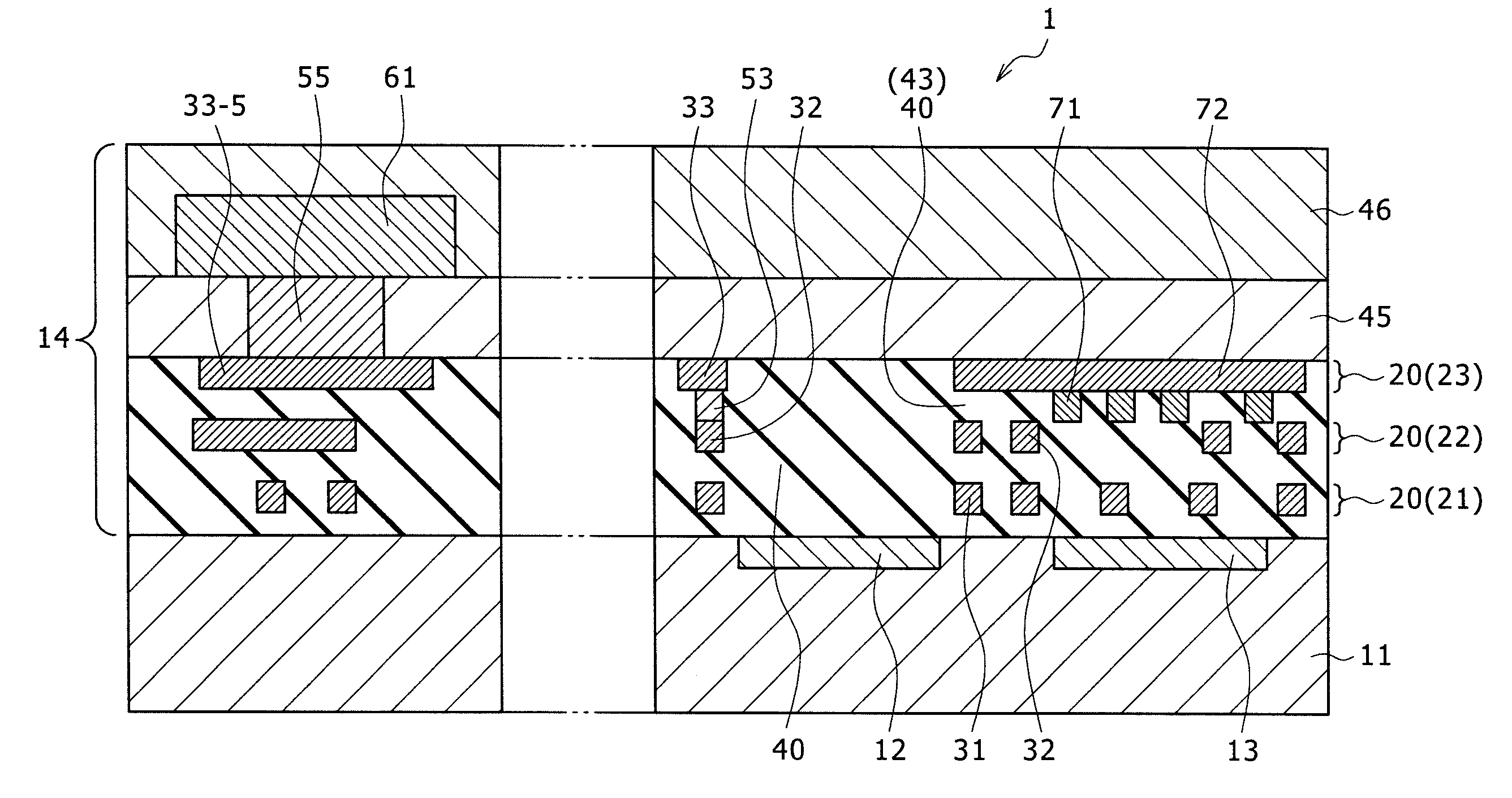
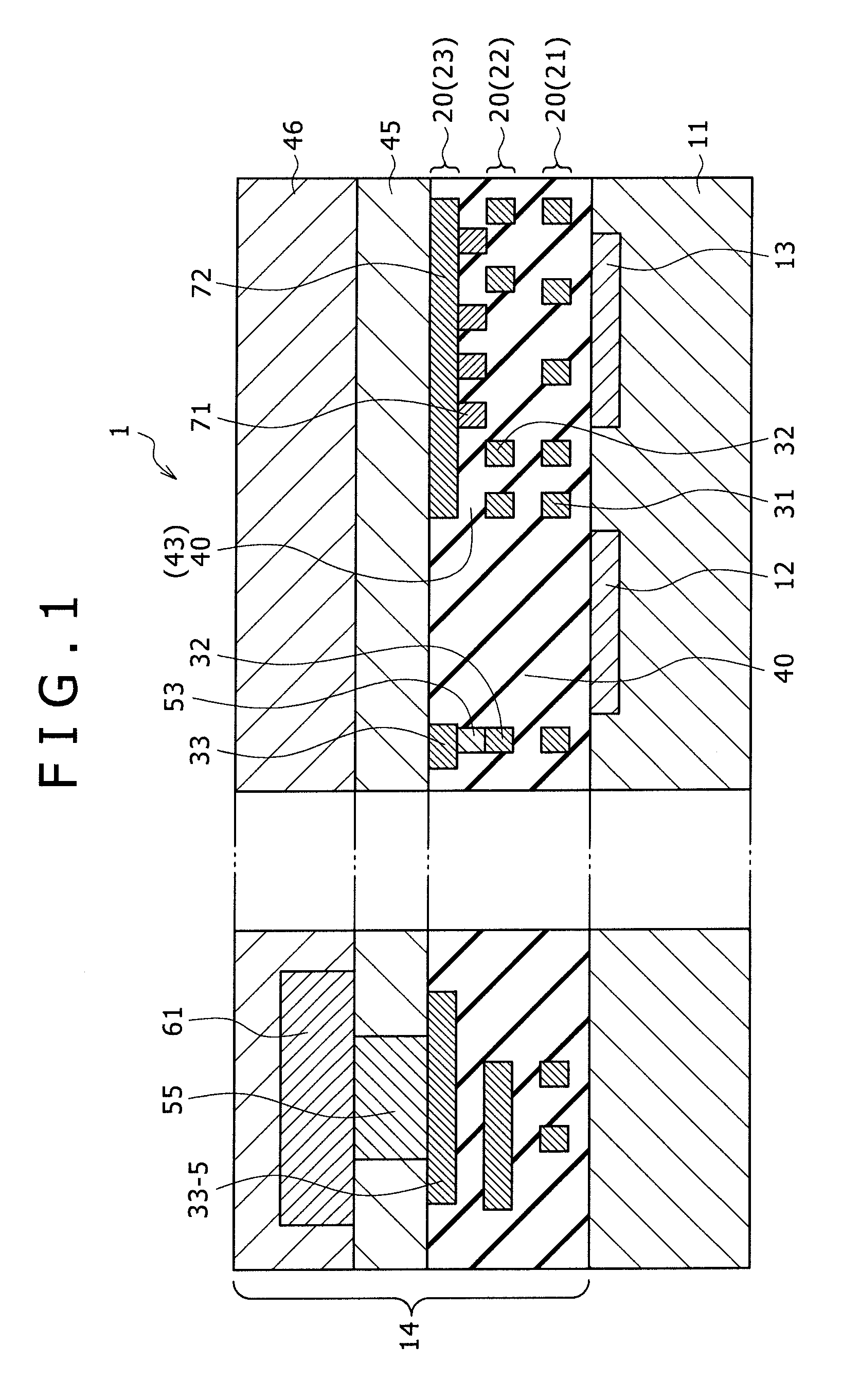
[0067]The first light-blocking film 71 may be formed with either line patterns or dot patterns. The line patterns may have either a uniform width or various widths. One example of the line patterns with various line widths will be described later as the present invention.
[0068]Similarly, the dot patterns may have either a uniform size or various sizes.
[0069]The surface of the interlayer insulating film 46 is planarized. Alternatively, a planarization insulating film (not shown) is formed on the interlayer insulating film 46. A color filter layer is formed on the interlayer insulating film 46 or the planarization insulating film although not shown in the drawing. Furthermore, a condensing lens is formed above each of the light-receiving pixel part 12 and the black-level reference pixel part 13 through a transparent insulating film.
[0070]The condensing lens formed above the light-receiving pixel part 12 condenses incident light and guides the light to the light-receiving pixel part 12...
first embodiment
[0071]In the first embodiment relating to the first solid-state imaging device, the imaging device has the first light-blocking film 71 formed above the areas among the second metal interconnects 32 of the second metal interconnect layer 22 and the second light-blocking film 72 that is connected to the first light-blocking film 71 and formed of the third metal interconnect layer 23 over the second metal interconnect layer 22. Therefore, the light-blocking films are formed in two layers. Thus, a light-blocking structure having thickness larger than that of the related-art light-blocking film is formed. This sufficiently ensures the light blocking above the black-level reference pixel part 13 and can enhance the light-blocking capability. In addition, because the light-blocking films are formed of a layer between the metal interconnect layers and the metal interconnect layer, an additional metal layer for the light-blocking film does not need to be formed. Therefore, it is possible to...
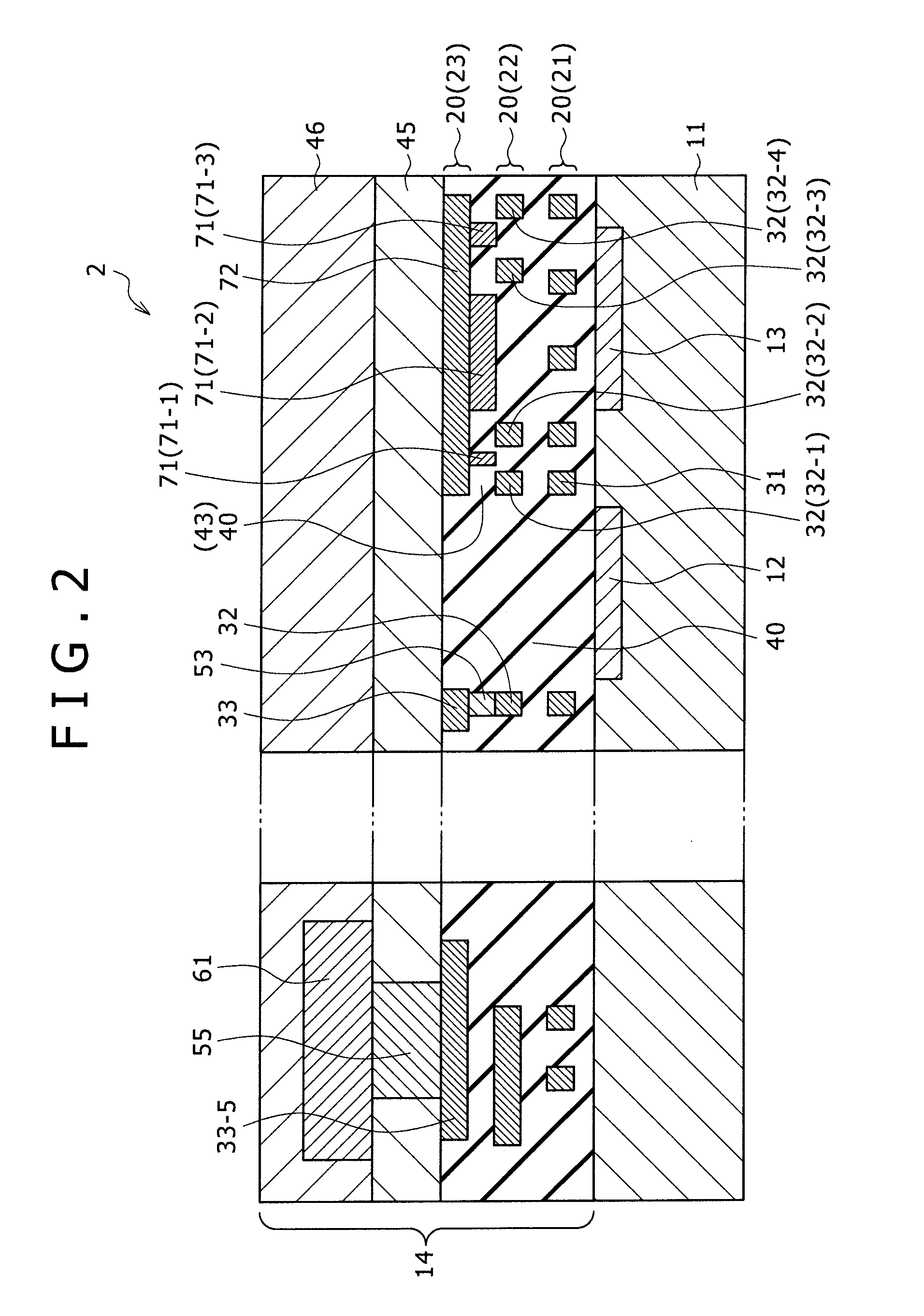
third embodiment
[0100]In the third embodiment relating to the first solid-state imaging device, the imaging device has the first light-blocking film 71 formed above the areas among the second metal interconnects 32 of the second metal interconnect layer 22 and the second light-blocking film 72 that is connected to the first light-blocking film 71 and formed of the third metal interconnect layer 23 over the second metal interconnect layer 22. Therefore, the light-blocking films are formed in two layers. Thus, a light-blocking structure having thickness larger than that of the related-art light-blocking film is formed. This sufficiently ensures the light blocking above the black-level reference pixel part 13 and can enhance the light-blocking capability. In addition, because the light-blocking films are formed of a layer between the metal interconnect layers and the metal interconnect layer, an additional metal layer for the light-blocking film does not need to be formed. Therefore, it is possible to...
PUM
 Abstract
Description
Claims
Application Information