Boundary acoustic wave device

a acoustic wave and device technology, applied in piezoelectric/electrostrictive/magnetostrictive devices, piezoelectric/electrostriction/magnetostriction machines, electrical equipment, etc., can solve the problem that the thickness of the idt electrode the surface of the siosub>2 /sub>layer cannot be prevented, and the idt electrode thickness increases the height of irregularities. a

Inactive Publication Date: 2009-07-30
MURATA MFG CO LTD
View PDF11 Cites 25 Cited by
  • Summary
  • Abstract
  • Description
  • Claims
  • Application Information

AI Technical Summary

Benefits of technology

[0009]To overcome the problems described above, preferred embodiments of the present invention provide a boundary acoustic wave device which includes electrodes having reduced thickness, which can confine an SH-type boundary acoustic wave between a piezoelectric body and a dielectric body, and which has low loss.
[0015]In the boundary acoustic wave device according to the first preferred embodiment, the electrodes are preferably formed by filling the grooves, which are provided in the upper surface of the LiNbO3 substrate, with the metal material and the dielectric layer is provided over the LiNbO3 substrate and the electrodes, and the thickness of the electrodes can be adjusted by varying the depth of the grooves. Therefore, there is substantially no unevenness between electrode-bearing portions and electrode-free portions. Thus, the upper surface of the dielectric layer can be readily planarized and the insertion loss can be reduced.
[0016]In addition, the metal material used to define the electrodes is preferably at least one of the metal materials of the first group, those of the second group, and those of the third group and θ of the Euler angles of the LiNbO3 substrate, the thickness of the dielectric layer, and the thickness of the electrodes are within any of the ranges shown in Table 1. Therefore, as shown in the experiments described below, an SH-type boundary acoustic wave can be non-leaky even if the electrodes have a reduced thickness. Thus, a boundary acoustic wave device which utilizes a SH-type boundary acoustic wave and which has low loss can be provided.
[0017]When the thickness of the electrodes, θ of the Euler angles, and the thickness of the dielectric layer are any of those shown in Table 2, the loss of the boundary acoustic wave device can be further reduced.
[0018]According to the second preferred embodiment, the electrodes are formed preferably by filling the grooves, which are formed in the upper surface of the LiTaO3 substrate, with the metal material and the dielectric layer is provided over the LiNbO3 substrate and the electrodes, and there is substantially no unevenness between electrode-bearing portions and electrode-free portions. Thus, the upper surface of the dielectric layer is flat or substantially flat and the insertion loss can be reduced. In addition, the material used to define the electrodes is preferably at least one of metal materials such as Al, Cu, Au, Ta, and Pt and the thickness of the electrodes, θ of the Euler angles of the LiTaO3 substrate, and the thickness of the dielectric layer are within any of the ranges shown in Table 2. Therefore, an SH-type boundary acoustic wave can be non-leaky even if the electrodes have a reduced thickness. Thus, a boundary acoustic wave device which utilizes a SH-type boundary acoustic wave and which has low loss can be provided.
[0019]In particular, when the thickness of the electrodes, θ of the Euler angles, and the thickness of the dielectric layer are within any of the ranges shown in Table 4, the loss of the boundary acoustic wave device can be further reduced.

Problems solved by technology

That is, a surface of the SiO2 layer cannot be prevented from having differences in height between the IDT electrodes and spaces therebetween.
Therefore, there is a problem in that surface irregularities of the SiO2 layer cause a deterioration of insertion loss.
An increase in the thickness of the IDT electrodes necessarily increases the height of the irregularities.
Therefore, the thickness of the IDT electrodes cannot be increased.
Therefore, it has been difficult to manufacture boundary acoustic wave devices having good frequency properties with high reproducibility.

Method used


Image

  • Boundary acoustic wave device
  • Boundary acoustic wave device
  • Boundary acoustic wave device

Examples


Embodiment Construction

[0045]Preferred embodiments of the present invention will be described below with reference to the accompanying drawings

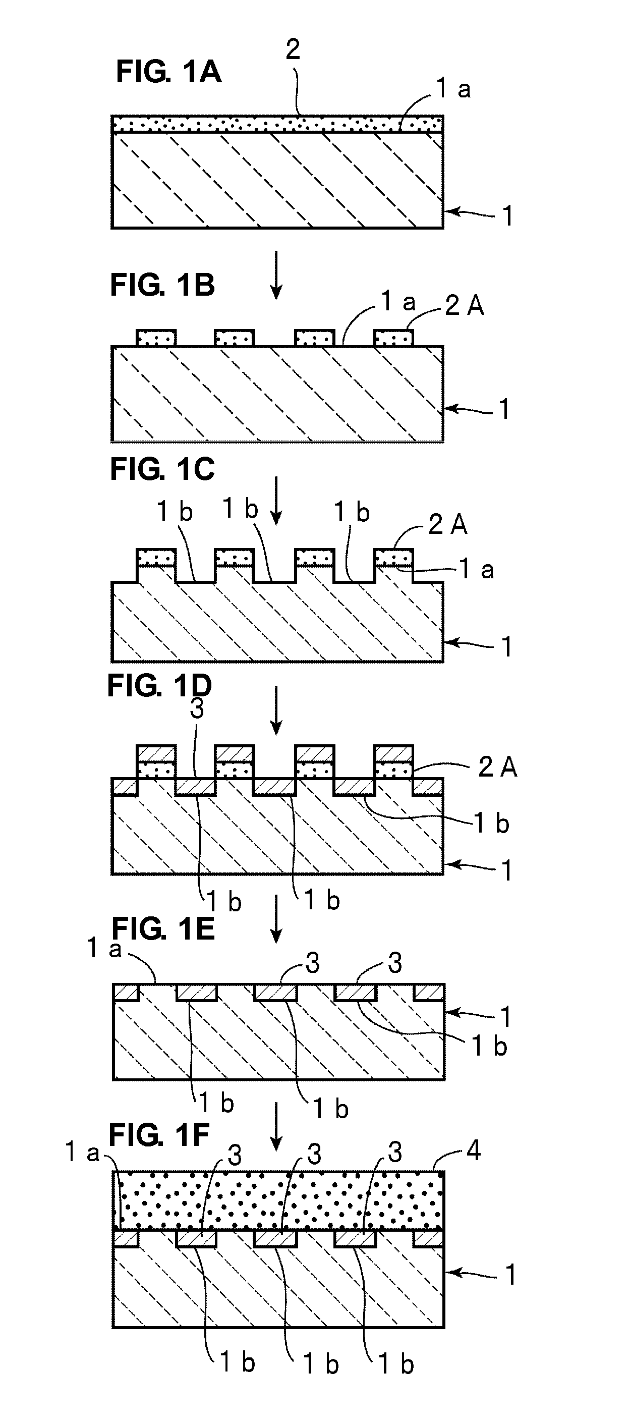
[0046]A method for manufacturing a boundary acoustic wave device according to a preferred embodiment of the present invention is described below with reference to FIGS. 1A to 1F.

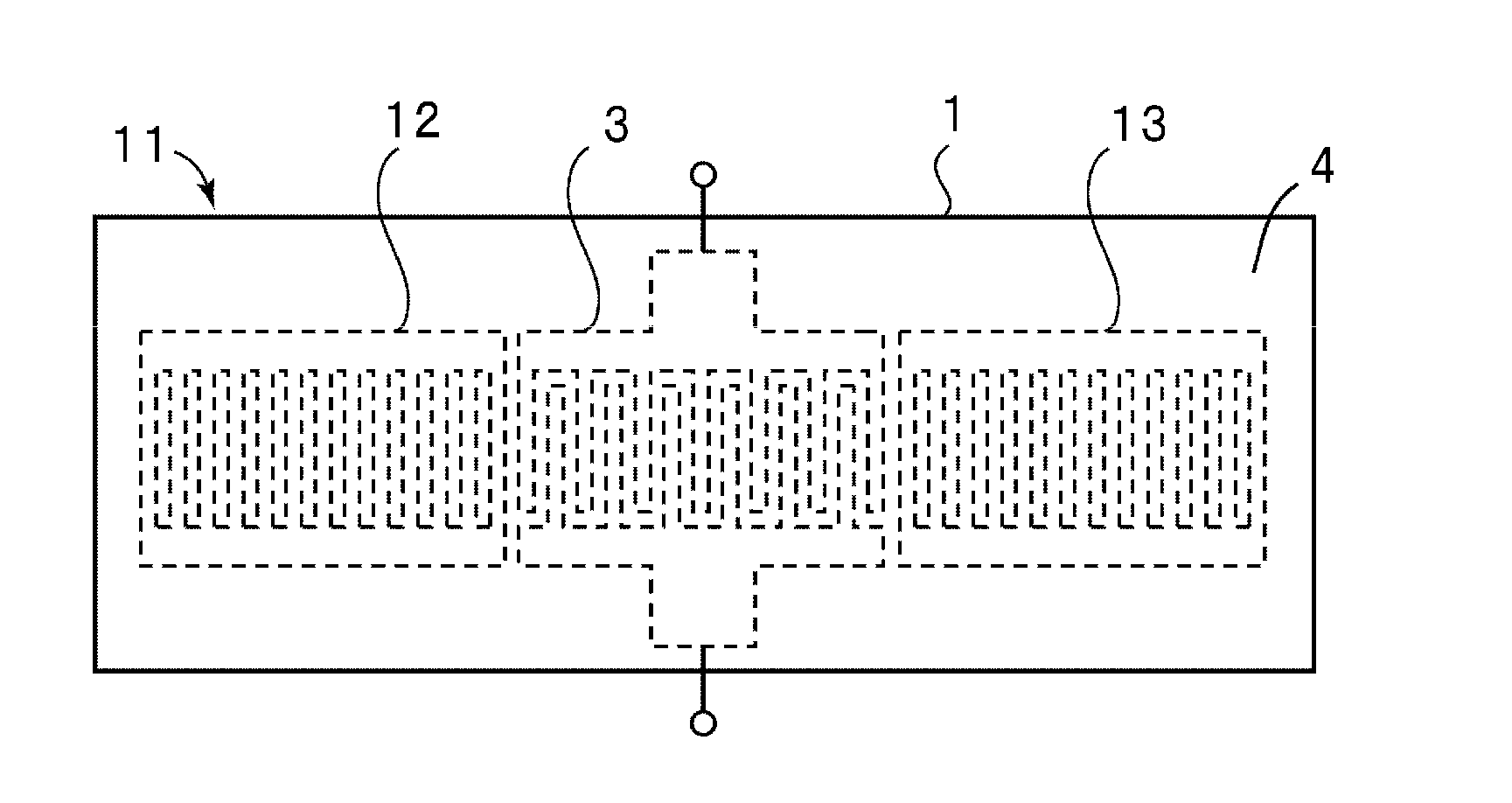
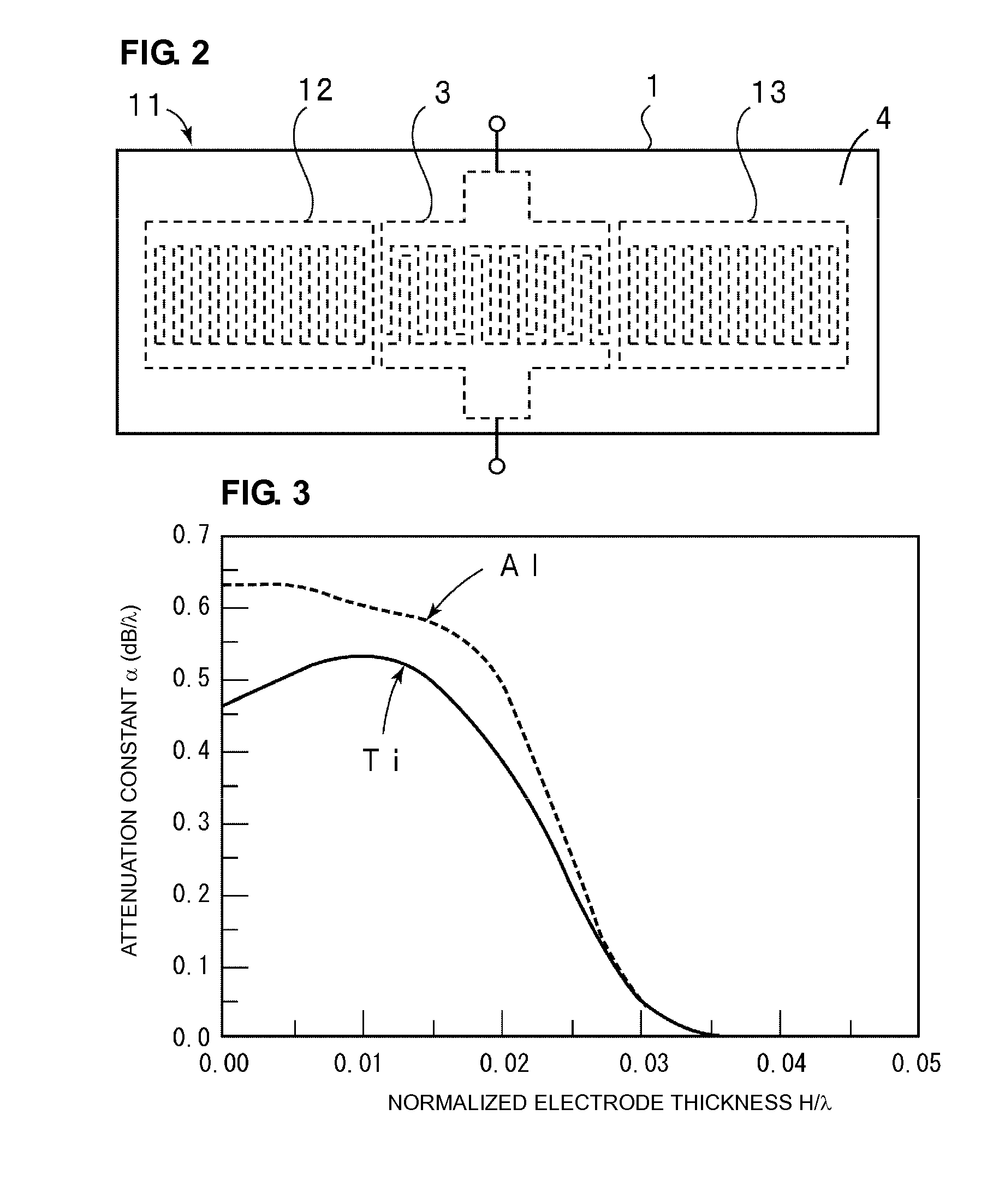
[0047]As shown in FIGS. 1A and 1A, a LiNbO3 substrate defining a piezoelectric substrate is prepared.

[0048]A photoresist layer 2 is formed over the upper surface 1a of the LiNbO3 substrate 1. The photoresist layer 2 can preferably be formed from any photoresist material that is resistant to reactive ion etching (RIE) which is performed later. In this example, a positive resist, AZ-1500™, available from Clariant (Japan) K. K., for example, is preferably used. In this example, the thickness of the photoresist layer 2 is preferably about 2 μm.

[0049]The photoresist layer 2 is patterned such that the photoresist layer is exposed to light and then developed, whereby a photoresist pattern 2A is fo...


PUM


Abstract

A boundary acoustic wave device includes a LiNbO3 substrate having a plurality of grooves provided in the upper surface thereof, electrode layers which are defined by a metal material filled in the grooves and which include IDT electrodes, and a dielectric layer, such as a SiO2 layer, provided over the upper surface of the piezoelectric substrate and the electrodes. The upper surface of the dielectric layer is flat or substantially flat. The thickness of the electrodes, θ of the Euler angles (0°, θ, −45° to +45°) of the LiNbO3 substrate, and the thickness of the dielectric layer are within any of the ranges shown in Table 1.

Description

BACKGROUND OF THE INVENTION[0001]1. Field of the Invention[0002]The present invention relates to boundary acoustic wave devices used as, for example, resonators or band-pass filters, and particularly, to a boundary acoustic wave device including a piezoelectric body, an electrode defined by a metal embedded in the upper surface of the piezoelectric body, and a dielectric body extending over the piezoelectric body and the electrode.[0003]2. Description of the Related Art[0004]Duplexers (DPXs) and RF filters used in mobile communication systems need to have both broad band-pass properties and good temperature properties. Conventional boundary acoustic wave devices used for such DPXs or RF filters include a piezoelectric substrate made of 36-50 degrees rotated Y-plate X-propagation LiTaO3. The piezoelectric substrate has a temperature coefficient of frequency of −45 ppm / ° C. to −35 ppm / ° C. A known technique for improving temperature properties is to arrange a SiO2 layer having a posit...

Claims


Application Information

Patent Timeline
Patent Type & Authority Applications(United States)
IPC IPC(8): H01L41/047
CPCH03H3/08H03H9/0222H03H9/02834H03H9/02661H03H9/02559H03H9/145H03H9/25H10N30/20H10N30/85
Inventor KADOTA, MICHIOKIMURA, TETSUYA
Owner MURATA MFG CO LTD
Why Eureka
Try Eureka