Semiconductor device, method of manufacturing thereof, signal transmission/reception method using such semiconductor device, and tester apparatus

Active Publication Date: 2009-07-30
RENESAS ELECTRONICS CORP
View PDF6 Cites 7 Cited by
  • Summary
  • Abstract
  • Description
  • Claims
  • Application Information

AI Technical Summary

Benefits of technology

[0027]According to the present invention, increase in chip size can be suppressed when s

Problems solved by technology

However, the pad is scratched by a needle of the probe during a probe test, which causes poor connection in bonding the pad later, or, which causes contamination due to shavings of the pad.
Further, as the chip size decreases and as the number of pads per chip increases, the pad size and the pitch between the pads decrease, and thus, satisfactory electrical connection between multiple pads and corresponding multiple probe needles becomes difficult accordingly.
However, in order to carr

Method used


Image

  • Semiconductor device, method of manufacturing thereof, signal transmission/reception method using such semiconductor device, and tester apparatus
  • Semiconductor device, method of manufacturing thereof, signal transmission/reception method using such semiconductor device, and tester apparatus
  • Semiconductor device, method of manufacturing thereof, signal transmission/reception method using such semiconductor device, and tester apparatus

Examples


first embodiment

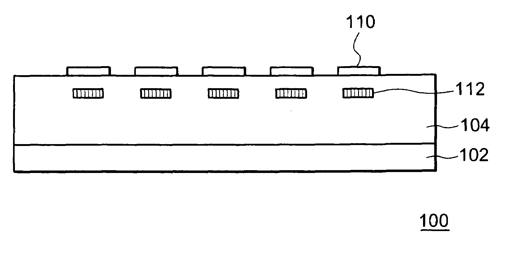
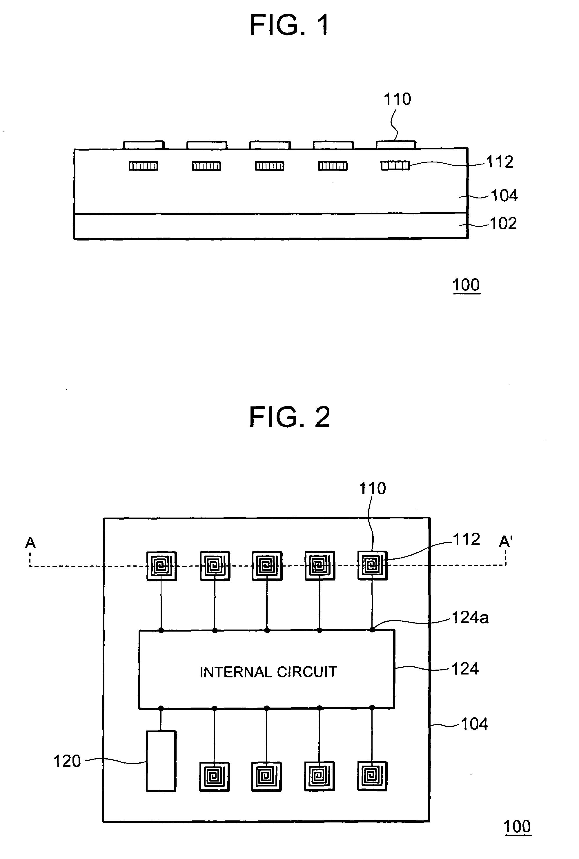
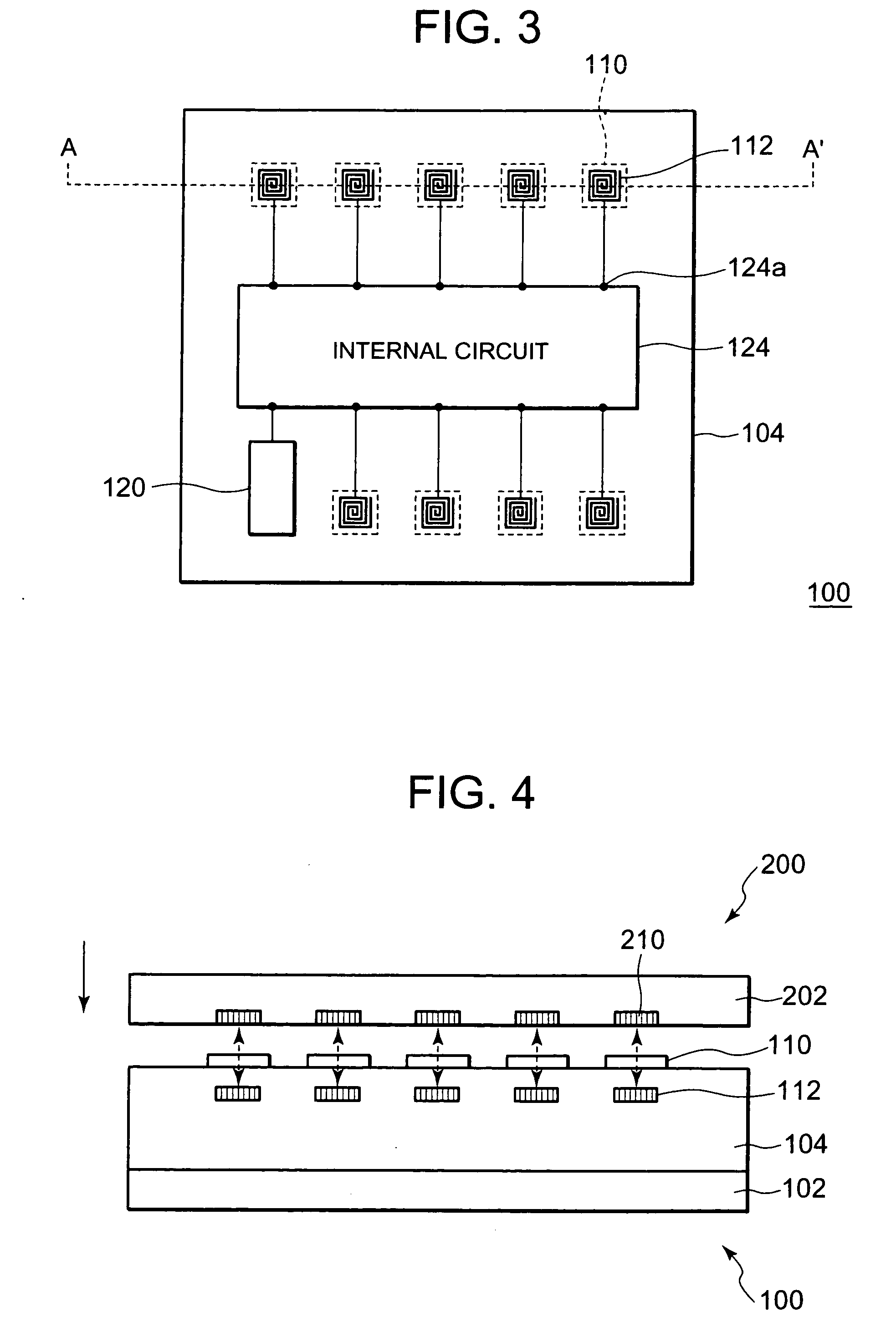
[0042]FIGS. 1 to 3 illustrate an exemplary structure of a semiconductor device 100 according to the present invention. FIG. 1 is a sectional view of the semiconductor device 100 and FIGS. 2 and 3 are plan views of the semiconductor device 100. FIG. 1 is a sectional view taken along the line A-A′ of FIG. 2 and FIG. 3.

[0043]As illustrated in FIG. 1, the semiconductor device 100 includes a semiconductor substrate 102 (substrate) and an insulating film 104 provided on the semiconductor substrate 102. The semiconductor device 100 also includes inductors 112 (first signal transmitting / receiving portion) provided in the insulating film 104 on the semiconductor substrate 102, and bonding pads 110 provided above the semiconductor substrate 102 so as to be superimposed on the inductors 112. Here, the semiconductor device 100 may be in a state before the semiconductor substrate 102 is divided into chips. The semiconductor substrate 102 may be, for example, a semiconductor wafer such as a silic...

second embodiment

[0067]FIG. 6 is a sectional view illustrating an exemplary structure of a semiconductor device 100 according to the present invention.

[0068]This embodiment is different from the embodiment described with reference to FIGS. 1 to 5 in that a plurality of inductors are provided under each of the bonding pads 110.

[0069]An inductor 112c, an inductor 112b, and an inductor 112a are stacked above the semiconductor substrate 102 in this order. The inductor 112c, the inductor 112b, and the inductor 112a may be inductors which are independent of one another such that phases of signals detected by the respective inductors are different from one another. Here, a plurality of inductors (inductor 112c, inductor 112b, and inductor 112a) are provided similarly under each of the bonding pads 110.

[0070]FIG. 7 is a sectional view illustrating a structure of a tester 200 for supplying a signal to the semiconductor device 100 and the semiconductor device 100 according to the second embodiment of the pres...

third embodiment

[0074]FIG. 8A is a sectional view illustrating an exemplary structure of a semiconductor device 100 according to the present invention.

[0075]In this embodiment, a plurality of inductors are provided below each of the bonding pads 110 similarly to the case illustrated in FIG. 6, but this embodiment is different from the embodiment described with reference to FIG. 6 in that the inductors are provided at locations shifted from one another in the plan view.

[0076]FIG. 8B is a sectional view illustrating a structure of a tester 200 for supplying a signal to the semiconductor device 100 according to the third embodiment of the present invention.

[0077]When the semiconductor device 100 has the structure as illustrated in FIG. 8A, inductors of the tester 200 are provided at locations corresponding to the inductor 112a, the inductor 112b, and the inductor 112c of the semiconductor device 100, which are shifted from one another in the plan view. Here, the inductor 210c on the tester side, the i...


PUM


Abstract

A semiconductor device (100) includes: a substrate (102); a bonding pad (110) provided above the substrate (102); and an inductor (112) provided above the substrate (102) and below the bonding pad (110) for carrying out signal transmission/reception to/from the external in a non-contact manner by electromagnetic induction.

Description

BACKGROUND OF THE INVENTION[0001]1. Field of the Invention[0002]The present invention relates to a semiconductor device, a method of manufacturing thereof, a signal transmission / reception method using such a semiconductor device, and a tester apparatus.[0003]2. Description of Related Art[0004]In recent years, semiconductor devices are known which conduct data communication by wireless communication.[0005]Japanese Patent Application Laid-open No. 2007-134694 discloses a semiconductor device for communicating data by an electromagnetic induction system. The semiconductor device has a coil antenna and a semiconductor integrated circuit connected to the coil antenna. When a coil antenna connected to a reader / writer is brought close to the semiconductor device, the coil antenna connected to the reader / writer generates an AC magnetic field. The AC magnetic field penetrates the coil antenna in the semiconductor device. An electromotive force is generated between terminals of the antenna by...

Claims


Application Information

Patent Timeline
IPC IPC(8): G09F25/00H01L29/82H01L21/50G01R31/26
CPCG01R31/2886G01R31/3025H01L2924/30107H01L2924/10253H01L28/10G01R31/303H01L23/48H01L23/645H01L24/05H01L24/48H01L2924/01004H01L2924/14H01L2924/19042H01L2924/19043H01L2924/3025H01L2224/48H01L2924/00H01L2924/00014H01L2224/45099H01L2224/45015H01L2924/207
Inventor NAKASHIBA, YASUTAKA
Owner RENESAS ELECTRONICS CORP
Why Eureka
Try Eureka