Local stress engineering for CMOS devices

a technology of local stress engineering and cmos, which is applied in the direction of semiconductor devices, electrical equipment, basic electric elements, etc., can solve the problems of difficult integration of sige source/drain region and silicon-carbon source/drain region

Active Publication Date: 2009-07-30
GLOBALFOUNDRIES US INC
View PDF13 Cites 38 Cited by
  • Summary
  • Abstract
  • Description
  • Claims
  • Application Information

AI Technical Summary

Problems solved by technology

However, the integration of both SiGe source/drain regions and silicon-carbon source/drain regions is challenging since SiGe s

Method used


Image

  • Local stress engineering for CMOS devices
  • Local stress engineering for CMOS devices
  • Local stress engineering for CMOS devices

Examples


Embodiment Construction

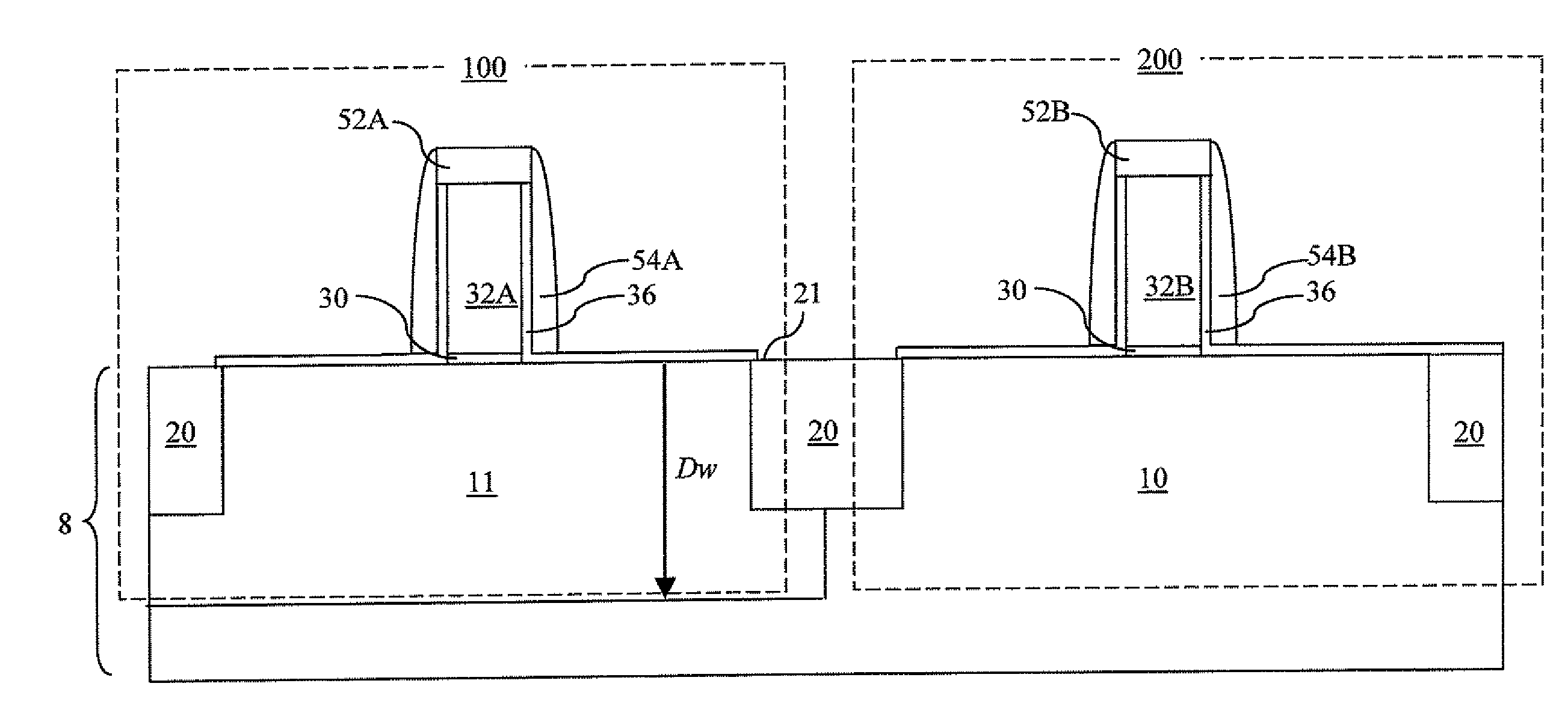
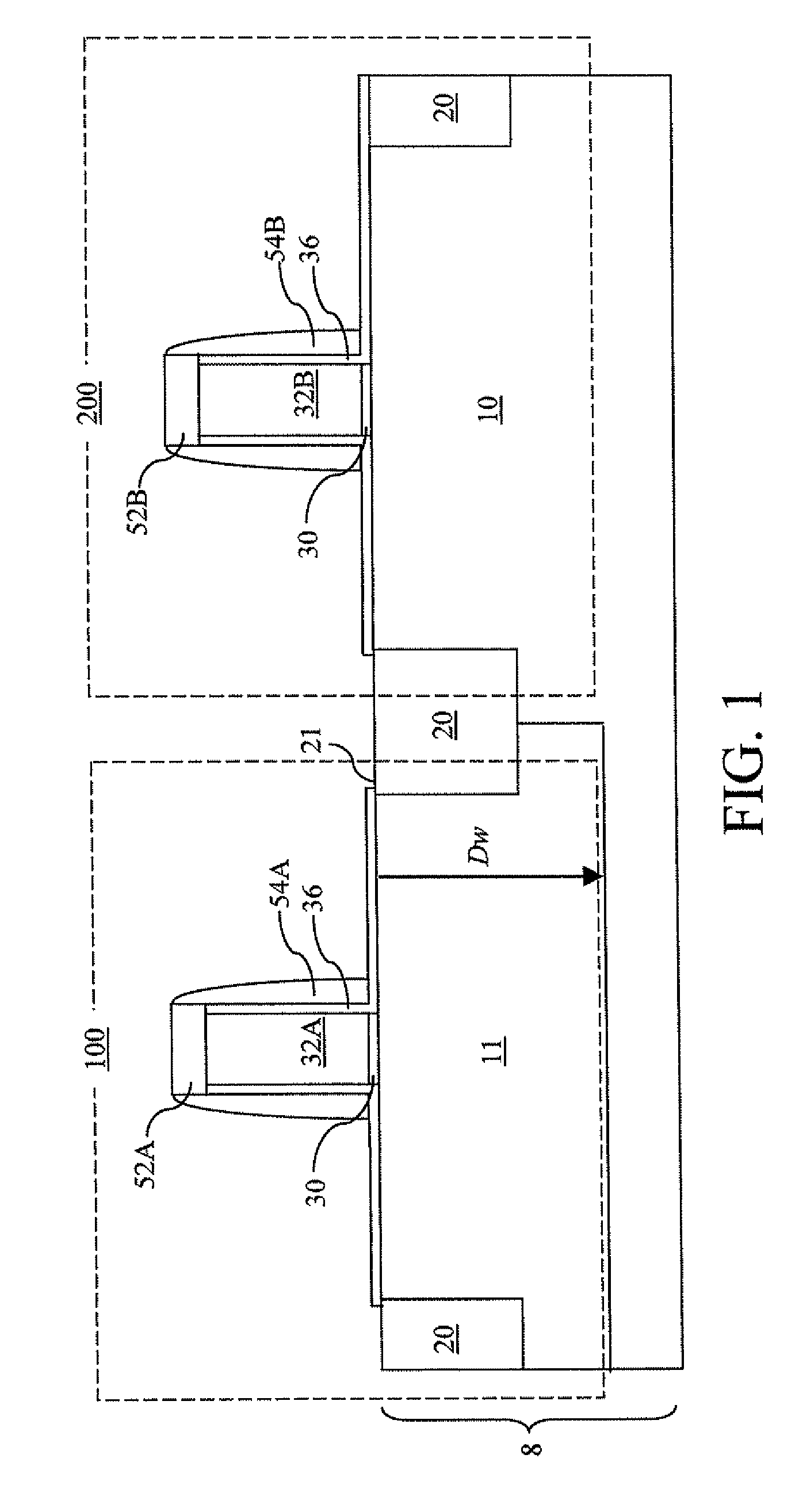
[0040]As stated above, the present invention relates to methods for forming semiconductor devices that include an n-type field effect transistor (NFET) having embedded SiC source / drain regions and a p-type field effect transistor having embedded SiGe source / drain regions, which are now described in detail with accompanying figures. It is noted that like and corresponding elements are referred to by like reference numerals.

[0041]Referring to FIG. 1, a first exemplary semiconductor structure according to a first embodiment of the present invention is shown, which comprises a semiconductor substrate 8 containing a first semiconductor region 10 and a shallow trench isolation structure 20. The first semiconductor region 10 comprises a semiconductor material having a doping of a first conductivity type at a first dopant concentration. The semiconductor substrate 8 further contains a second semiconductor region 11 comprising the semiconductor material and having a doping of a second conduc...


PUM


Abstract

A first dielectric layer is formed over a PFET gate and an NFET gate, and lithographically patterned to expose a PFET area, while covering an NFET area. Exposed PFET active area is etched and refilled with a SiGe alloy, which applies a uniaxial compressive stress to a PFET channel. A second dielectric layer is formed over the PFET gate and the NFET gate, and lithographically patterned to expose the NFET area, while covering the PFET area. Exposed NFET active area is etched and refilled with a silicon-carbon alloy, which applies a uniaxial tensile stress to an NFET channel. Dopants may be introduced into the SiGe and silicon-carbon regions by in-situ doping or by ion implantation.

Description

FIELD OF THE INVENTION[0001]The present invention relates to methods for forming semiconductor devices, and more particularly, to methods for forming semiconductor devices that include an n-type field effect transistor (NFET) having embedded SiC source / drain regions and a p-type field effect transistor having embedded SiGe source / drain regions, wherein the PFET has enhanced hole mobility and the NFET has enhanced electron mobility.BACKGROUND OF THE INVENTION[0002]Various techniques for enhancing semiconductor device performance through manipulation of carrier mobility have been investigated in the semiconductor industry. One of the key elements in this class of technology is the manipulation of stress in the channel of transistor devices by employing lattice mismatched materials in source / drain regions. Such lattice mismatched materials may be advantageously employed to generate stress on a semiconductor device, for example, by applying biaxial stress or uniaxial stress in a channel...

Claims


Application Information

Patent Timeline
IPC IPC(8): H01L21/8236
CPCH01L21/823807H01L29/7848H01L21/823814
Inventor OUYANG, QIQINGSCHONENBERG, KATHRYN T.
Owner GLOBALFOUNDRIES US INC
Why Eureka
Try Eureka