Electronic microscope apparatus

a microscope and electronic technology, applied in the direction of instruments, material analysis using wave/particle radiation, heat measurement, etc., can solve the problems of small low intensity of detected characteristic x-rays, and limited deterioration of the spatial resolution of the element image, so as to achieve high spatial resolution and high s/n

Active Publication Date: 2009-08-06
HITACHI HIGH-TECH CORP
View PDF5 Cites 23 Cited by
  • Summary
  • Abstract
  • Description
  • Claims
  • Application Information

AI Technical Summary

Benefits of technology

[0017]Processing according to the present invention enables provision of an electronic microscope apparatus capable of measuring an elastically scattered elect

Problems solved by technology

However, the intensity of detected characteristic X-rays is low and, therefore, there is a need to scan the specimen with the electron beam for several ten minutes to several hours.
Because a long time is thus required for measurement, a specimen drift correction is made by using an elastically scattered electron image and it is necessary to intermit measurement of characteristic X-rays several times to several ten times. A specimen drift during characteristic X-rays measurement causes a deterioration of the spatial resolution of the element image.
With respect to this point, if the number of times a specimen drift correction is made is increased, the deterioration of the spatial resolution of the element image can be limited to a small degree, but the meas

Method used


Image

  • Electronic microscope apparatus
  • Electronic microscope apparatus
  • Electronic microscope apparatus

Examples


first embodiment

[0054](1) Configuration of Scanning Transmission Electron Microscope

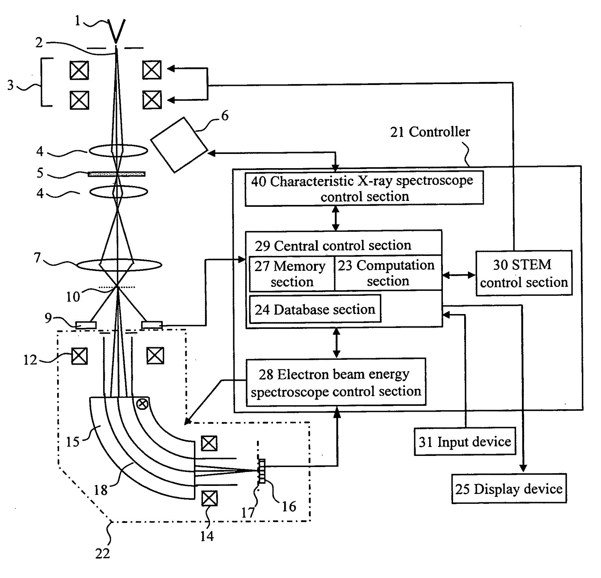
[0055]FIG. 1 is a diagram schematically showing a configuration of essential portions of a scanning transmission electron microscope (STEM) having a characteristic X-ray spectrometer and an electron beam energy analyzer (EELS) according to an embodiment of the present invention. This scanning transmission electron microscope is common to the embodiments.

[0056]An electron beam 2 generated in an electron beam source 1 forms a probe by means of an objective lens 4 and the probe is applied to a specimen 5. The position at which the electron beam is applied to the specimen 5 is deflected by electron beam scanning coils 3. Characteristic X-rays are generated from the specimen to which the electron beam is applied, and are detected by a characteristic X-ray spectrometer 6. The electron beam passing through the specimen 5 forms an object point 10 on an electron beam energy analyzer 22 by means of a projection lens 7. The el...

second embodiment

[0077](1) Difference from First Embodiment

[0078]In the first embodiment, energy filter images are obtained and an element image is obtained by using the three sorts of filter images (F1 to F3) (see FIG. 3). In the second embodiment, data from which an element image is obtained by the electron beam energy analyzer (EELS) 22 is not the energy filter images. That is, an EELS spectrum itself is first obtained and the background is extrapolated from the spectrum data to obtain the intensity of the core loss. The EELS spectrum in the second embodiment is a detailed one such that a spectrum shape such as shown in FIG. 4B can be identified. A detailed spectrum is measured with respect to each pixel of an image. On the other hand, in the first embodiment, data in F1, F2, and F3 has a signal intensity through an energy width (ΔE) (FIG. 4A) and a detailed spectrum is not measured.

[0079]In the first embodiment, energy filter images are measured and an EELS-based element image is obtained on the...

third embodiment

[0086](1) Element Image Observation

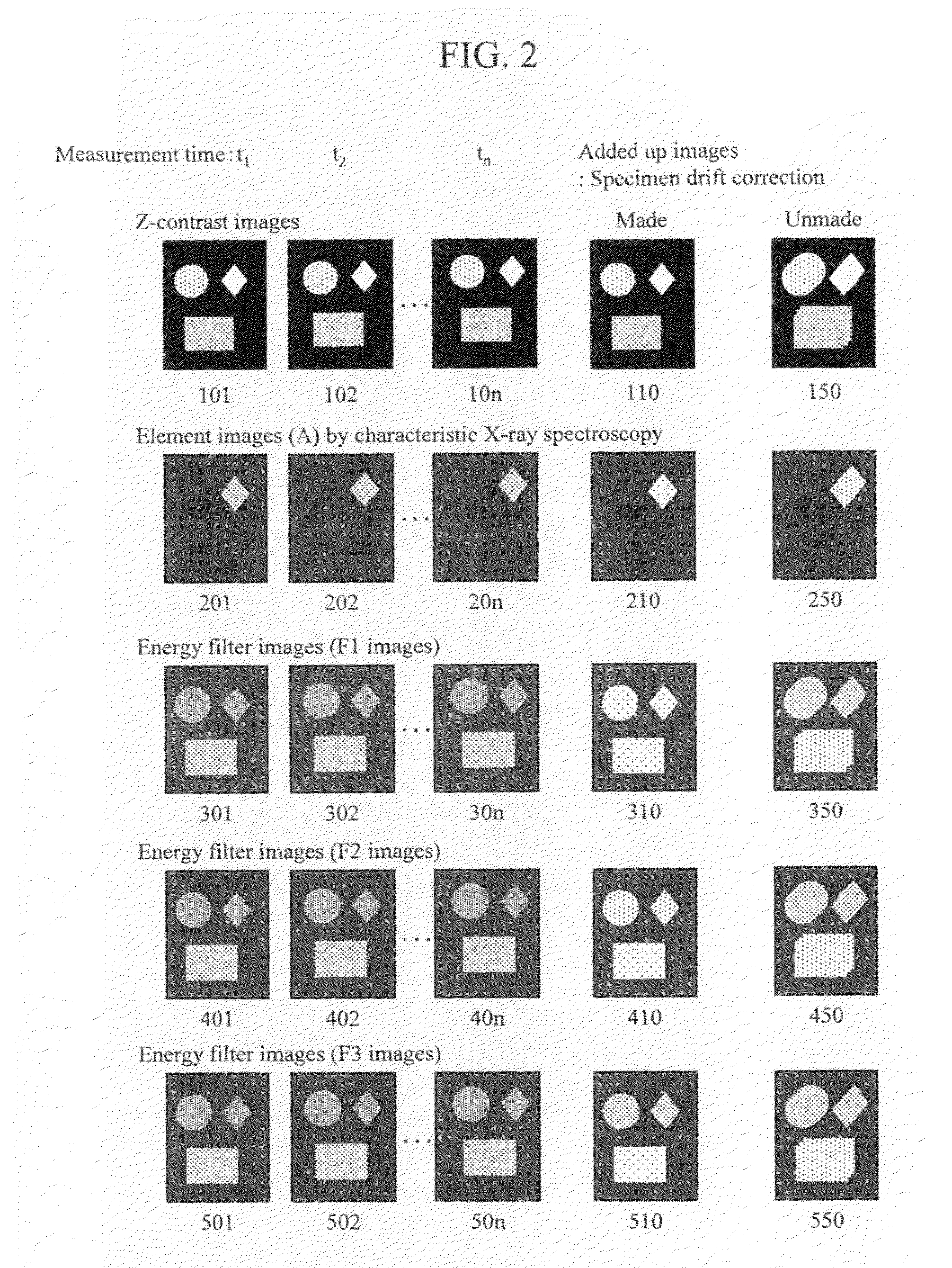
[0087]FIG. 6 is a diagram for explaining a technique for element image observation according to the third embodiment of the present invention.

[0088]Also in the third embodiment, in the same way as in the first embodiment, elastically scattered electrons from the specimen 5 are detected by the Z-contrast detector 9 in correspondence with the electron beam application position to form a Z-contrast image 1001. Also, simultaneously with the Z-contrast image, an element image (A) by the characteristic X-ray spectrometer (see FIG. 2 because it is omitted in FIG. 6) and an energy filter image (F1) 3001 by the electron beam energy analyzer (see FIG. 2 because energy filter images (F2, F3) are omitted in FIG. 6) are observed. These five sorts of images are the results of image forming on the basis of detection of elastically scattered electrons, characteristic X-rays and energy loss electrons with the detectors performed when the electron beam is applied to...


PUM


Abstract

To enable measurement of an elastically scattered electron image, a characteristic-X-ray-based element image and an electron-beam-energy-spectroscopy-based element image with a high S/N and high spatial resolution in an electronic microscope having a function to produce an element image. Measurement of a characteristic X-ray signal and electron beam energy loss spectra or measurement of a plurality of energy filter signals including a core loss of an observed element is performed simultaneously and continuously with detection of elastically scattered electrons transmitted through a specimen to be analyzed, and element images based on characteristic X-rays and electron beam energy spectroscopy are added up while correcting a positional misalignment with respect to elastically scattered electron images continuously observed (see FIG. 1).

Description

BACKGROUND OF THE INVENTION[0001]1. Field of the Invention[0002]The present invention relates to an electronic microscope apparatus having a function to measure an element image of a specimen.[0003]2. Background Art[0004]As a result of making semiconductor elements and magnetic head elements finer and smaller in size, such elements have a structure in which thin films of several nanometers are stacked in a region on the submicron order. In the development of elements, it is important to analyze the structure of such a minuscule region and an element distribution in such a region. Devices for performing elemental analysis include a characteristic X-ray spectrometer and an electron beam energy analyzer (also called an energy filter), which are attached to transmission electron microscopes (TEM) or scanning transmission electron microscopes (STEM) for observing and designating a minuscule region.[0005]In a case where an element image with a good S / N is observed by using a characteristi...

Claims


Application Information

Patent Timeline
IPC IPC(8): G01N23/00
CPCH01J37/244H01J37/265H01J37/28H01J2237/24455H01J2237/24475H01J2237/2807H01J2237/24564H01J2237/24578H01J2237/24585H01J2237/2485H01J2237/2805H01J2237/24485
Inventor KAJI, KATZUTOSHI
Owner HITACHI HIGH-TECH CORP
Why Eureka
Try Eureka