Vertical fin-fet mos devices

a technology of vertical fins and mos, which is applied in the field of vertical mos devices, can solve the problems of large complexity involved, large size tends to work against performance, and large volume, and achieves the effect of low contact resistan

Active Publication Date: 2009-08-13
GLOBALFOUNDRIES US INC
View PDF6 Cites 104 Cited by
  • Summary
  • Abstract
  • Description
  • Claims
  • Application Information

AI Technical Summary

Benefits of technology

[0007]The present inventive technique produces high-density, vertical Fin-FET devices with low contact resistance by means of vertical silicon “fins” that act as the transistor body. Doped source and drain regions are formed at the bottoms and tops, respectively, of the fins. Gate structures are formed along sidewalls of the fins, spanning the vertical distance between the source and drain regions and separated from the fins by thin gate insulators. Current flows vertically through the channel region between the source and drain regions when an appropriate bias is applied to the gates. Through the use of selective doping, both nFET and pFET variants of the inventive vertical Fin-FET device are easily formed on the same substrate. Preferably, the substrate is an SOI (silicon-on-insulator) wafer, but any suitable substrate or portion thereof having a silicon layer formed over an insulator layer (e.g., buried oxide layer—“BOX”) could be employed.

Problems solved by technology

As MOS device size decreases, tremendous challenges arise in a variety of areas, including source / drain contact resistance and current carrying capacity.
In these two areas at least, extremely small size tends to work against performance.
However, there is considerable process complexity involved in forming the second, buried gate and in connecting to it, and the planar double-gate transistor is not significantly different from conventional planar transistor structures in terms of its ability to be scaled.
Such planar devices are rapidly approaching the physical limits of scaling.
Series resistance in Fin-FETs is a significant problem, however.

Method used


Image

  • Vertical fin-fet mos devices
  • Vertical fin-fet mos devices
  • Vertical fin-fet mos devices

Examples


Embodiment Construction

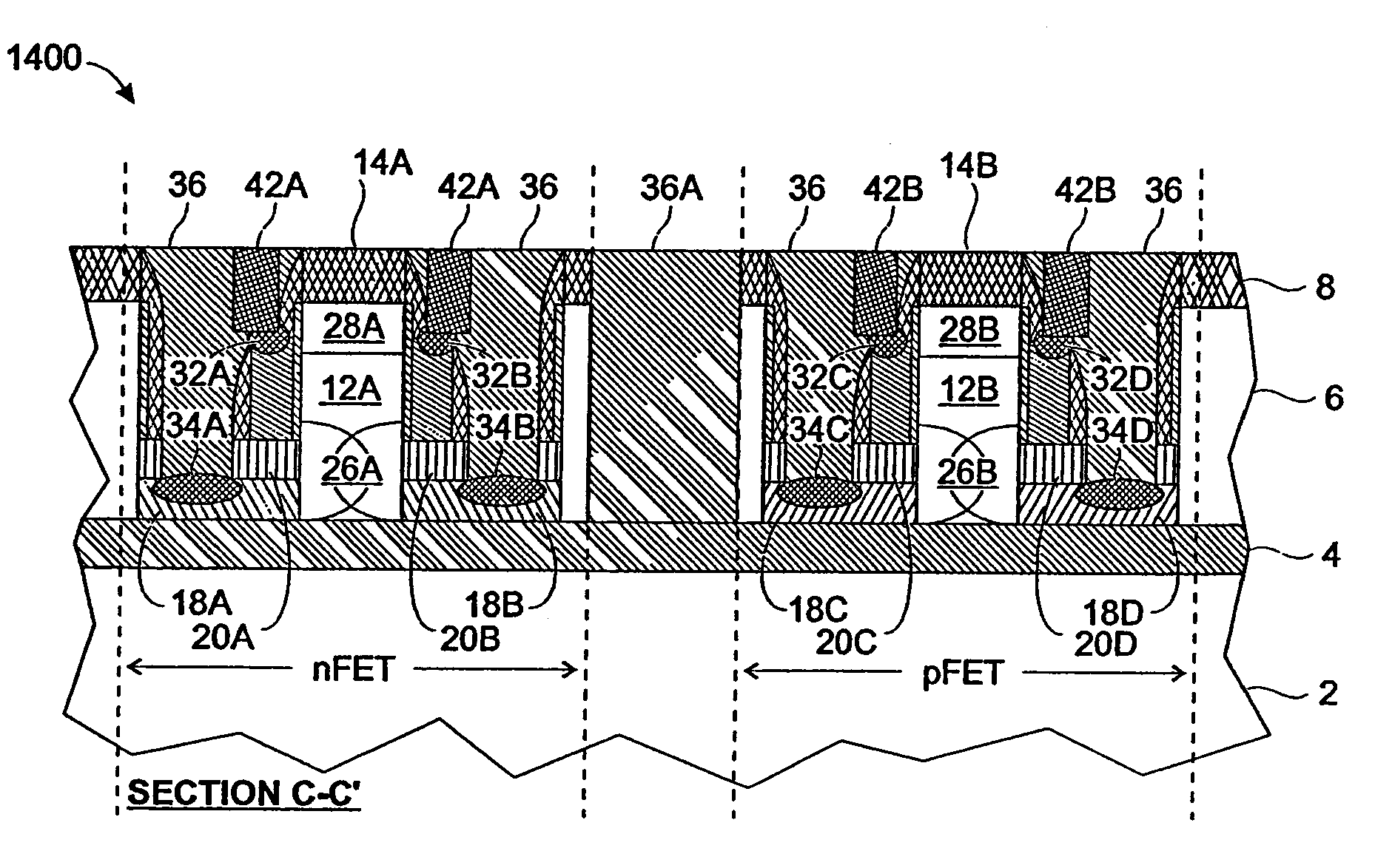
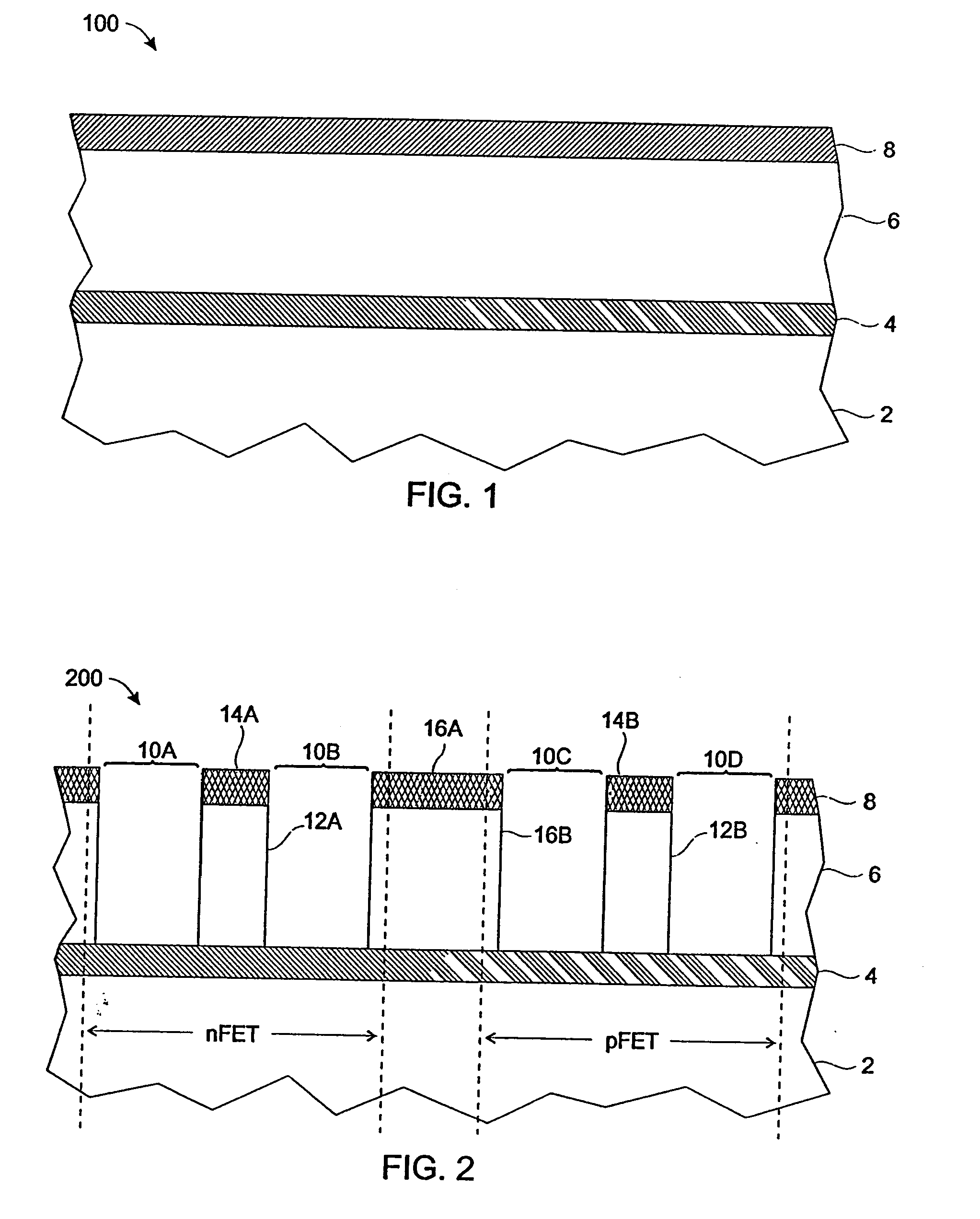
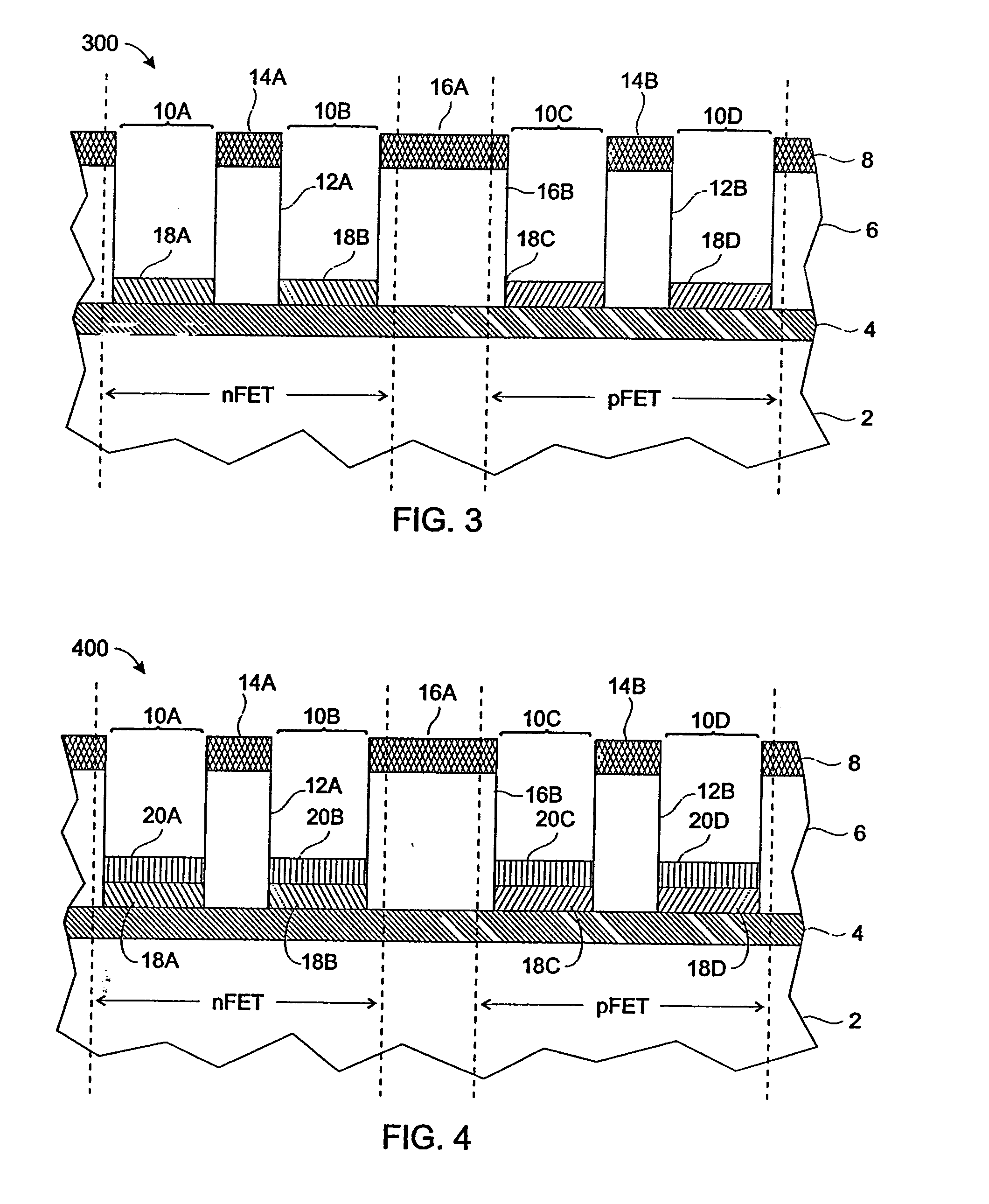
[0039]The present inventive technique produces high-density, vertical Fin-FET devices with low contact resistance by forming tall, thin vertical silicon “fins” that act as the transistor body. Appropriately doped source and drain regions are formed at the bottoms and tops, respectively, of the fins and gate structures are formed along sidewalls of the fins, overlapping the doped source and drain regions, thereby creating a vertical channel region in the fin between the source and drain regions. Current flows vertically through channels that form in the channel region adjacent to the gate structures and extending between the source and drain regions when an appropriate bias is applied to the gates. Through the use of selective doping, both nFET and pFET variants of the inventive vertical Fin-FET device are easily formed on the same substrate. Preferably, the substrate is an SOI (silicon-on-insulator) wafer, but any suitable substrate or portion thereof having a silicon layer formed o...


PUM


Abstract

A new class of high-density, vertical Fin-FET devices that exhibit low contact resistance is described. These vertical Fin-FET devices have vertical silicon “fins” (12A) that act as the transistor body. Doped source and drain regions (26A, 28A) are formed at the bottoms and tops, respectively, of the fins (12A). Gates (24A, 24B) are formed along sidewalls of the fins. Current flows vertically through the fins (12A) between the source and drain regions (26A, 28A) when an appropriate bias is applied to the gates (24A, 24B). An integrated process for forming pFET, nFET, multi-fin, single-fin, multi-gate and double-gate vertical Fin-FETs simultaneously is described.

Description

TECHNICAL FIELD OF THE INVENTION[0001]The present invention relates generally to semiconductor devices, more particularly to MOSFET (Metal-Oxide-Semiconductor Field Effect Transistor) devices, and still more particularly to vertical MOSFETs.BACKGROUND OF THE INVENTION[0002]In 1965, Dr. Gordon Moore, then Director of Research and Development for Fairchild Semiconductor, made the observation that the number of transistor devices per integrated circuit had been doubling every couple of years since the creation of the first integrated circuits in the late 1950's and that he expected the trend to continue for the foreseeable future. This observation was dubbed “Moore's Law” by the trade press. Now almost 40 years later, despite numerous dire predictions of fundamental obstacles, unrelenting industry efforts towards every-increasing semiconductor density have effectively affirmed Dr. Moore's prophetic observation, and the trend is still expected to continue unabated for the foreseeable fu...

Claims


Application Information

Patent Timeline
Patent Type & Authority Applications(United States)
IPC IPC(8): H01L29/78H01L21/336
CPCH01L29/78642H01L29/66787H01L21/2257
Inventor CHIDAMBARRAO, DURESETIBEINTNER, JOCHENDIVAKARUNI, RAMACHANDRA
Owner GLOBALFOUNDRIES US INC
Why Eureka
Try Eureka