Semiconductor device

Active Publication Date: 2009-08-13
KK TOSHIBA
View PDF2 Cites 31 Cited by
  • Summary
  • Abstract
  • Description
  • Claims
  • Application Information

AI Technical Summary

Benefits of technology

[0012]Since the oxide electrode of a Ti base in patent document 1 has a low stability as compared with the oxide of a Hf base or a Zr base, a possibility of giving oxygen to a gate dielectric film becomes high, and the effective work function of the gate electrode f

Problems solved by technology

When promoting a thin gate dielectric film, and to reach an EOT of a gate diel

Method used


Image

  • Semiconductor device
  • Semiconductor device
  • Semiconductor device

Examples


first embodiment

[0135]Next, a semiconductor device according to a first embodiment of the invention is described with reference to FIG. 13A to FIG. 13C.

[0136]The semiconductor device according to this embodiment includes an nMIS transistor and a pMIS transistor formed on a silicon substrate, and these MIS transistors are of the foregoing Type-A. Steps of manufacturing the semiconductor device of this embodiment are shown in FIG. 13A to FIG. 13C. The semiconductor according to this embodiment is formed in the following manner.

[0137]First of all FIG. 13A shows a device separating region 4 for separating a pMIS transistor forming region and an nMIS transistor forming region from each other on a semiconductor substrate, for example, a silicon substrate 2. This device separating region 4 is formed by means of, for example, an STI (shallow trench isolation) technology. This device separating region can also be formed by means of an LOCOS (local oxidation of silicon) technology.

[0138]Thereafter, a p-well ...

second embodiment

[0161]Next, a semiconductor device according to a second embodiment of the invention is described with reference to FIG. 18A to FIG. 18C.

[0162]A semiconductor device according to this embodiment includes an nMIS transistor and a pMIS transistor formed on a silicon substrate, and these MIS transistors are of the foregoing Type-B. Steps of manufacturing the semiconductor device of this embodiment are shown inFIG. 18A to FIG. 18C. The semiconductor according to this embodiment is formed in the following manner.

[0163]First of all, similar to the case of the first embodiment, a device separating region 4 is formed on a silicon substrate 2 (FIG. 18A). Thereafter, a p-well 6 is formed in the nMIS transistor forming region, and an n-well 8 is formed in the pMIS transistor forming region. Subsequently, in order to regulate the threshold voltage, impurities are introduced into the p-well 6 and the n-well 8.

[0164]Next, a gate dielectric film 40 is formed on the silicon substrate 2. This gate d...

third embodiment

[0177]Next, a semiconductor device according to a third embodiment of the invention is described with reference to FIG. 19A to FIG. 19C.

[0178]A semiconductor device according to this embodiment includes an nMIS transistor and a pMIS transistor on a silicon substrate, and these MIS transistors are of the foregoing Type-C. Steps of manufacturing the semiconductor device of this embodiment are shown in FIG. 19A to FIG. 19C. The semiconductor according to this embodiment is formed in the following manner.

[0179]First of all, similar to the first embodiment, a device separating region 4 is formed on a silicon substrate 2 (FIG. 19A). Thereafter, a p-well 6 is formed in the nMIS transistor forming region, and an n-well 8 is formed in the pMIS transistor forming region. Subsequently, in order to regulate the threshold voltage, impurities are introduced into the p-well 6 and the n-well 8.

[0180]Next, as shown in FIG. 19A, a gate dielectric film 50 is formed on the silicon substrate 2. This gat...


PUM


Abstract

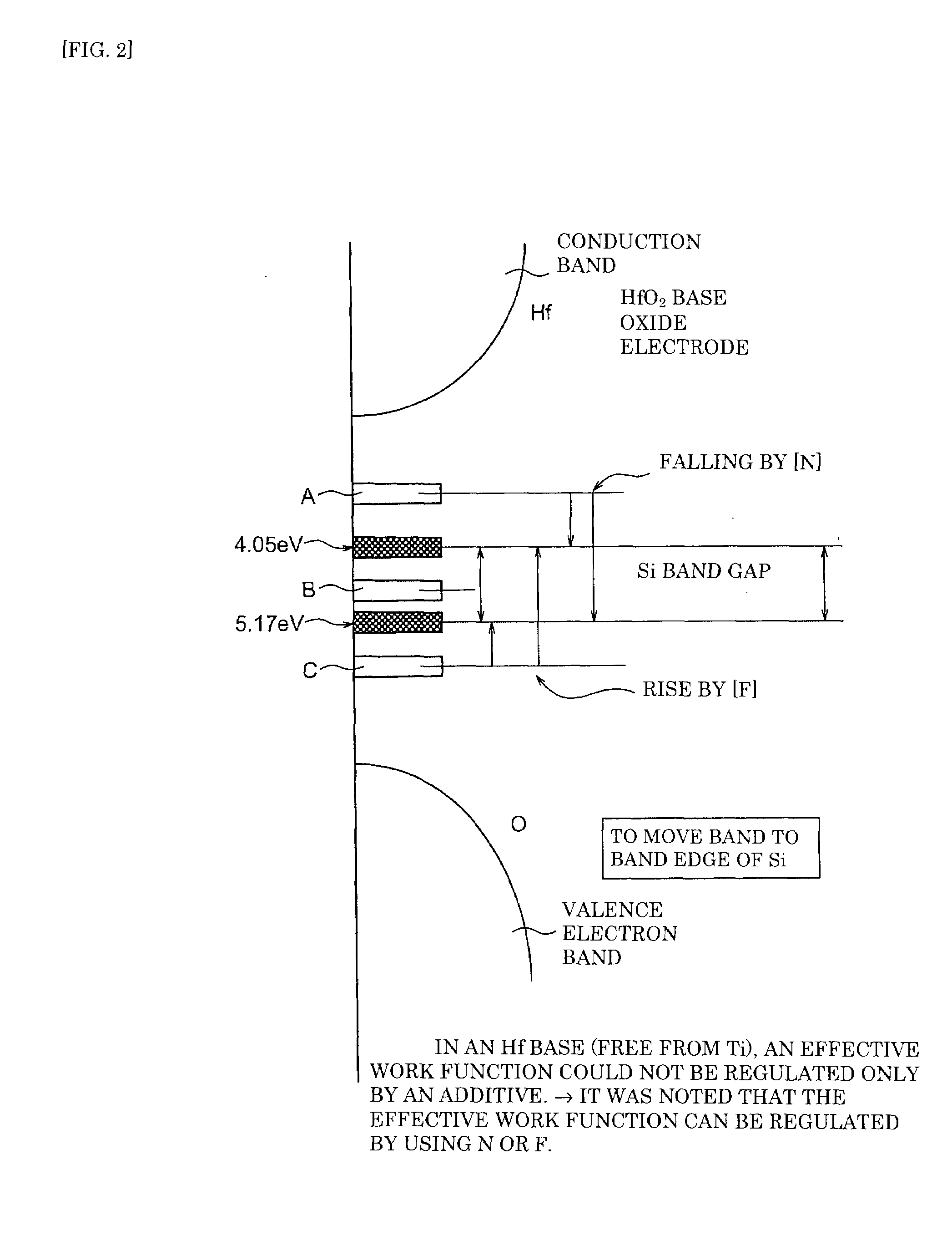
According to one embodiment, it is possible to provide a semiconductor device provided with an MIS transistor which has an effective work function being, as much as possible, suitable for low threshold operation. A CMIS device provided with an electrode having an optimal effective work function and enabling low threshold operation to achieve by producing an in-gap level by the addition of a high valence metal in an Hf (or Zr) oxide and changing a position of the in-gap level by nitrogen or fluorine or the like has been realized.

Description

CROSS-REFERENCE TO RELATED APPLICATIONS[0001]This application is based upon and claims the benefit of priority from prior Japanese Patent Application No. 2008-31770, filed Feb. 13, 2008, the entire contents of which are incorporated herein by reference.BACKGROUND[0002]1. Technical Field[0003]Exemplary embodiments described herein relate to a semiconductor device.[0004]2. Description of the Related Art[0005]Before, in order to secure the charge quantity induced by the channel of a MISFET (metal insulator semiconductor field effect transistor), a gate dielectric film has been decreased in thickness and a capacity has been enlarged.[0006]As the result, a thin gate dielectric film (SiO2 film) is promoted, and its thickness can be below 1 nm.[0007]However, when the gate electrode made of polycrystalline silicon is formed on the gate dielectric film made of SiO2, a depletion layer will arise in an interface with the gate dielectric film, and an Equivalent Oxide Thickness (EOT) of the gate...

Claims


Application Information

Patent Timeline
IPC IPC(8): H01L29/78
CPCH01L21/823842H01L29/785H01L27/1203H01L21/823857H01L21/823821
Inventor SHIMIZU, TATSUOKOYAMA, MASATO
Owner KK TOSHIBA
Why Eureka
Try Eureka