Crack Stop Trenches

a technology of crack stop and trenches, applied in the field of electrical devices, can solve the problems of additional challenges in maintaining yield and component reliability, affecting product yield and other reliability issues, and preventing delamination and other reliability issues

Active Publication Date: 2009-08-13
INFINEON TECH AG
View PDF11 Cites 32 Cited by
  • Summary
  • Abstract
  • Description
  • Claims
  • Application Information

AI Technical Summary

Benefits of technology

[0008]Embodiments of the invention include methods and a structure for preventing delamination and other reliability issues associated with chip dicing processes and chip package interactions. The method includes forming active regions disposed in cell regions of a substrate, the cell regions separated by dicing channels. Back end of line (BEOL) layers are formed in the cell regions and the dicing channels. Crack stop trenches are then formed encircling the cell regions by etching a portion of the BEOL layers surrounding the cell regions. The wafer is then diced along the dicing channels.

Problems solved by technology

One of the challenges in semiconductor technology requires developing technologies with good product yield and reliability.
Due to their poor mechanical properties, use of low-k and ultra-low dielectric constant materials introduces additional challenges in maintaining yield and component reliability.
Thus, what are needed in the art are semiconductor components containing low-k and ultra-low dielectric constant materials but without comprising product yield or component reliability.

Method used


Image

  • Crack Stop Trenches
  • Crack Stop Trenches
  • Crack Stop Trenches

Examples


Embodiment Construction

[0021]The making and using of the presently preferred embodiments are discussed in detail below. It should be appreciated, however, that the present invention provides many applicable inventive concepts that can be embodied in a wide variety of specific contexts. The specific embodiments discussed are merely illustrative of specific ways to make and use the invention, and do not limit the scope of the invention.

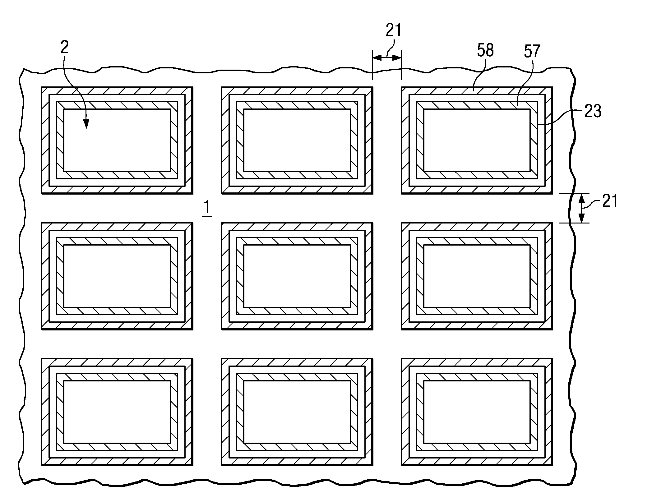
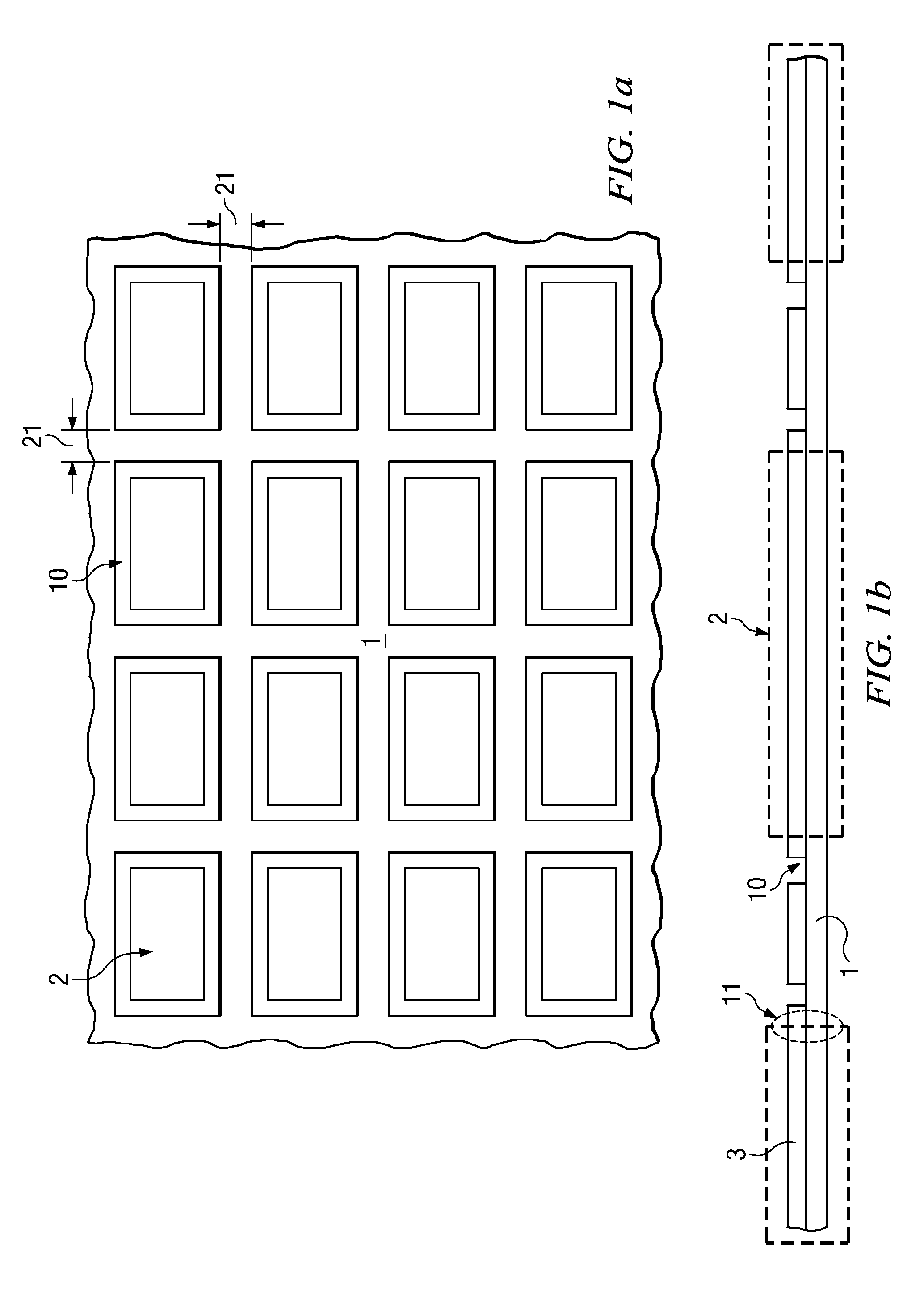
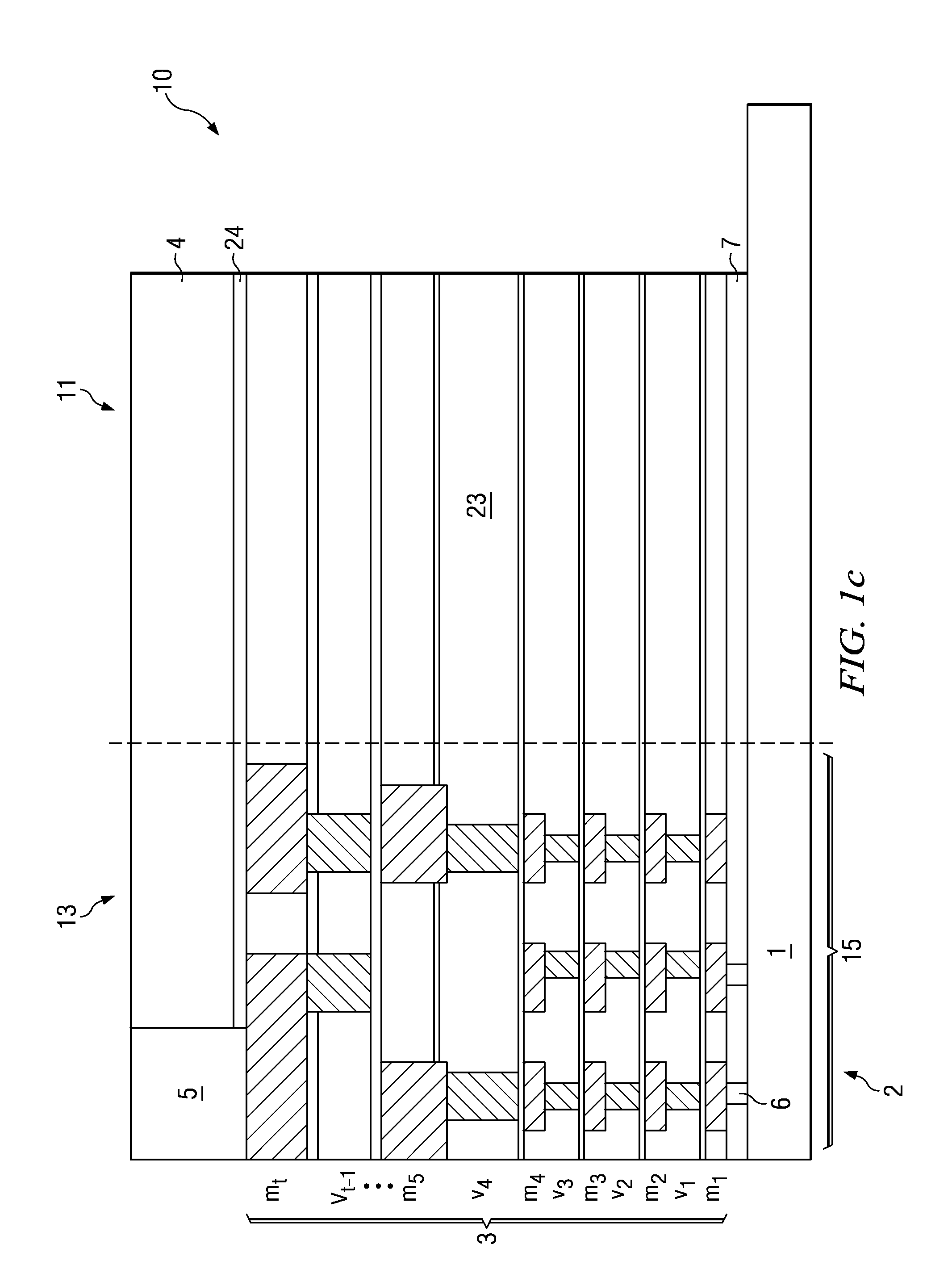
[0022]The present invention will be described with respect to preferred embodiments in a specific context, namely a structure and method for forming crack stop trenches. In various embodiments, the invention avoids the problems arising from delamination or failure of low-k or ULK dielectric layers during / after chip dicing.

[0023]Low-k dielectric materials are used to lower parasitic interconnect capacitances in BEOL or metallization levels. Recent and future technology will likely introduce further lower dielectric constant materials such as ultra low-k dielectric materials. H...


PUM


Abstract

Structures and methods of forming crack stop trenches are disclosed. The method includes forming active regions disposed in cell regions of a substrate, the cell regions separated by dicing channels, and forming back end of line (BEOL) layers over the substrate, the BEOL layers being formed over the cell regions and the dicing channels. Crack stop trenches are then formed encircling the cell regions by etching a portion of the BEOL layers surrounding the cell regions. The wafer is diced along the dicing channels.

Description

TECHNICAL FIELD[0001]This invention relates generally to electronic devices, and more particularly to crack stop trenches.BACKGROUND[0002]Semiconductor devices are used in many electronic and other applications. Semiconductor devices comprise integrated circuits that are formed on semiconductor wafers by depositing many types of thin films of material over the semiconductor wafers, and patterning the thin films of material to form the integrated circuits.[0003]Metallization layers are usually the top-most layers of semiconductor devices. The manufacturing of semiconductor devices is typically classified into two phases: the front end of line (FEOL) and the back end of line (BEOL). The BEOL is typically considered to be the point of the manufacturing process where metallization layers are formed, and the FEOL is considered to include the manufacturing processes prior to the formation of metallization layers.[0004]While some integrated circuits have a single top layer of metallization...

Claims


Application Information

Patent Timeline
Patent Type & Authority Applications(United States)
IPC IPC(8): H01L21/00
CPCH01L21/78H01L21/31116
Inventor KALTALIOGLU, ERDEMWENDT, HERMANN
Owner INFINEON TECH AG
Why Eureka
Try Eureka